Download
1 / 25
550 likes | 1.55k Vues
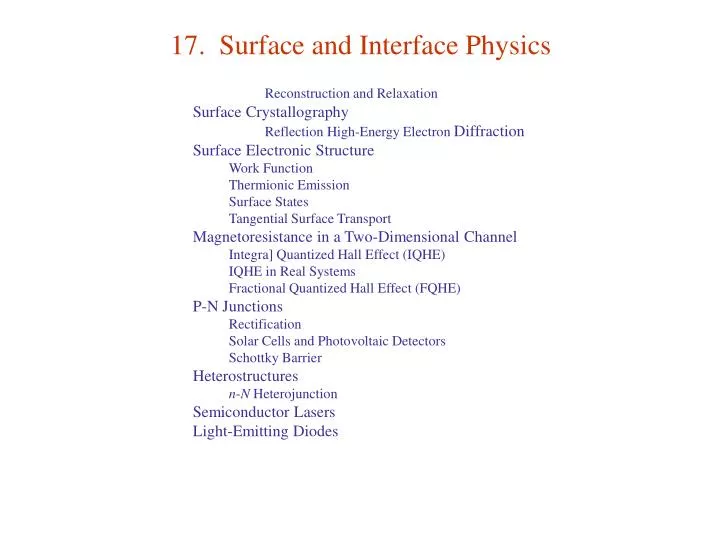
17. Surface and Interface Physics. Reconstruction and Relaxation Surface Crystallography Reflection High-Energy Electron Diffraction Surface Electronic Structure Work Function Thermionic Emission Surface States Tangential Surface Transport Magnetoresistance in a Two-Dimensional Channel

E N D
17. Surface and Interface Physics • Reconstruction and Relaxation • Surface Crystallography • Reflection High-Energy Electron Diffraction • Surface Electronic Structure • Work Function • Thermionic Emission • Surface States • Tangential Surface Transport • Magnetoresistance in a Two-Dimensional Channel • Integra] Quantized Hall Effect (IQHE) • IQHE in Real Systems • Fractional Quantized Hall Effect (FQHE) • P-N Junctions • Rectification • Solar Cells and Photovoltaic Detectors • Schottky Barrier • Heterostructures • n-N Heterojunction • Semiconductor Lasers • Light-Emitting Diodes
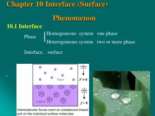
Reconstruction and Relaxation Dangling bonds in diamond Surface 3 outermost atomic layers. Unreconstructed surface: Outermost layer same as in bulk except for a contraction in interlayer distance. C.f., interatomic distances in molecules are smaller than those in solid. Reconstructed surface (occurs mostly in nonmetals): Bonding on surface rearranged to eliminate dangling bonds. Superstructure may (Si) or may not (GaAs) be formed. Surfaces of nominally high indices can be built up from low ibdex ones by steps. Attachment energies are low at steps, hence facilitate chemical activities.
Surface Crystallography 5 distinct 2-D nets: oblique, square, hexagonal, rectangular, & centered rectangular. Substrate net // surface is used as reference. E.g., for the (111) surface of a cubic substrate, the substrate net is hexagonal & the surface net is referred to these axes. Let c1, c2 be translational vectors for the surface mesh & a1, a2 be those for the substrate. If the angles of the 2 meshes are equal, Wood’s notation is often used: α is the angle of relative rotation between the meshes ( R α is omitted if α = 0 ).
p = primitive c = centered
Reciprocal lattice vectors cj* for the surface are defined by 31 c c* Reciprocal net points represented in 3-D as rods surface. Diffracted beam given by intercepts of Ewald sphere with rods.
Low Energy Electron Diffraction (LEED): E ~ 10-1k eV Pt (111) 51eV 63.5eV
Reflection High-Energy Electron Diffraction RHEED gracing angle Radius k of Ewald sphere for 100 keV e’s 103 A–1 >> 2π /a 1 A–1 . → Ewald sphere ~ flat plane → Intercept with rods ~ line
Surface Electronic Structure: Work Function Work functionWεvac – μ Operationally, the vacuum level εvac is the energy of an e more than 100A outside the metal. The chemical potential μ is often called the Fermi level. W depends on surface orientation because of the surface dipoles. Einstein relation for photoemission:
Thermionic Emission Consider an e-gas in vacuum in equilibrium with a metal. By definition: → Flux of e leaving metal when all e’s are drawn off is equal to the incident flux: Charge flux: Richardson-Dushman equation
Surface States Weak binding approximation: Let the outward normal to the surface be in the +x direction. s, x > 0 x < 0 ψ real → J = 0. ψin real only if k = G / 2. → s, q are determined by the conditions that ψ & ψ are continuous at the surface. The bound state energy ε is obtained by solving the 2-component secular equation.
Tangential Surface Transport Surface bound states affects the thermal distributions of e & h near surface ( μ shifted ). μ = same everywhere → band-bending. Surface highly conducting Inversion layer on n-type semiC. Accumulation layer on n-type semiC. Thickness & carrier conc nS of surface layer controlled by E → MOSFET b = mobility Prob 2
Magnetoresistance in a Two-Dimensional Channel The static magnetoconductivity tensor in 3D was obtained in Prob 6.9 as For a surface z-axis, we set → Alternatively, in a cross field Ey & Bz , we have from Chap 6 along x. In a frame moving with vD , e is stationary → there is extra field → In the lab frame,
Hall resistance jy = 0 → → σxx = σyy = 0 →
Integral Quantized Hall Effect (IQHE) • Vpp ~ 0 (σ* ~ ) at some Vg . • Plateaus in VH near such Vg . • VH / ISD = h / e2s at plateaus (IQHE) Strong field → Landau levels are either filled or empty If εF falls on a Landau level: Pauli Exclusion principle → only inelastic scattering possible. Low T → required phonons not available. → σ* ~ B = 18T. T = 1.5K. ISD = 1 μA. Explanation too simplified
IQHE in Real Systems Ideal crystal Real crystal Landau levels are broadened by impurities / defects in real crystals. Also, some Landau levels are partially filled unless εF = Landau level. Yet in the IQHE, ρH is accurately quantized in dirty samples & over a range of Vg. → Better model needed ( & provided by Laughlin ) Laughlin’s thought experiment: 2-D plane rolled into cylinder. →
In a dirty system, there’re 2 types of carrier states: • Extended states: continuous around loop. • Localized states: not continuous around loop. Extended & localized states do not coexist at the same E. • In the presence of Φ : • Extended states: enclose Φ → E changes with period δΦ = h c / e. • Localized states: do not enclose Φ → E not change; effect like gauge transformation. When εF falls in the localized states, all extended states below εF are filled both before & after a flux change δΦ. But an integral number N of e’s will be transferred (usually 1 e per Landau level). N is integral because the system is identical before & after the flux change. The corresponding energy change is δU = N e VH. →
Fractional Quantized Hall Effect (FQHE) FQHE: Hall effect with ρH quantized to fractional values.
p-n Junctions p-n junction = single crystal with different dopings. Interface may be less than 10–4 cm thick. Majority carriers will diffuse into the other side. The excess charges left behind set up an E field directed from n to p to oppose further diffusion. In equilibrium, μ for all carriers must be a constant everywhere. For h: unbiased junction For e: The absence of net current flow is accomplished in the junction by the exact cancelling between the generating and recombination current.
Rectification p-n junction in Ge Reverse biased: → Forward biased: → Similarly for holes. Well satisfied in Ge, but not so much in others.
Solar Cells and Photovoltaic Detectors Light with ω > Eg on p-n junction → e-h pair e-h pair diffused into junction: separated by built-in E → Forward voltage across junction (Photovoltaic effect)
Schottky Barrier Schottky barrier: metal-SemiC junction → → where x = 0 indicates the right-hand edge of barrier and the contact is at x = –xb . Let the potential at the contact be φ0 relative to the right-hand side: ε =16, eφ0 = 0.5 eV, n = 1016 cm–3 → xb = 0.3 μ m.
Heterostructures Heterostructures: Layers of 2 or more different semiC. → band structure design. Lattice mistmatch negligible → heterojunction = single crystal with different site occupancies across junction E.g., Ge / GaAs ( a 5.65A ) GaAs / Ge 3 types of band edge offsets: Good matches: AlAs / GaAs InAs / GaSb GaP / Si ZnSe / GaAs GaAs / (Al,Ga)As Both e & h are on the right GaSb / InAs
n-N Heterojunction Junction similar to Schottky barrier. Quantum well created for e on n-side. If n is lightly doped, impurity scattering will be negligible in well → mobility limited by lattice scattering, which falls off sharply for low T. E.g., μ 107 cm2 V–1 s–1 observed in GaAs / (Al,Ga)As. If thickness of N is reduced below depletion layer thickness, all e conduction // interface will be on the n side. ( high mobility e on n-side separated from their donors on N-side ) → 2-D e-gas, high-speed FET, …
Semiconductor Lasers Direct gap well Inversion condition (in well): Structure itself is an EM cavity ( flat // ends: radiation emitted in plane of junction ) (Al,Ga)As / GaAs / (Al,Ga)As pn GaAs: 8383A (1.48eV, near IR) 50% power to light conversion efficiency. 90% differential efficiency for small changes. For optical fibre transmissions Gax In1-x Py As1–y are used to minimize loss.
Light-Emitting Diodes In GaAs, inter-band photon are absorbed within 1 μm (strong absorption). The direct gap ternary GaAs1–xPx shortens λ with increasing x. → 1st visible (red) LED. Blue LED uses InxGa1–xN – AlyGa1–y N.