Download
1 / 27
270 likes | 401 Vues
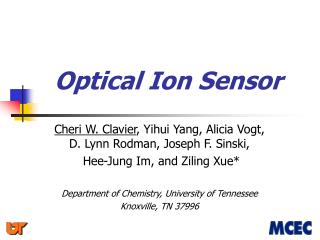
Integrated Nanoscale Ion-Channel Sensor. AgCl Electrode. Oxide. SU-8 Resist. Si. Project Goals. develop conceptual design for an all-silicon chip that allows freestanding lipid bilayer support fabricate a prototype of that chip investigate the influence of

E N D
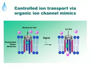
AgCl Electrode Oxide SU-8 Resist Si Project Goals • develop conceptual design for • an all-silicon chip that allows • freestanding lipid bilayer support • fabricate a prototype of that chip • investigate the influence of • surface modification layers on • bilayer Gigaseal formation • test channel insertion into • supported membrane • evaluate properties of planar • integrated AgCl electrodes Lipid Bilayer with Ion Channels Important building blocks of a fully integrated biosensor with on-chip sensing and signal processing
Technical Approach For the fabrication … Challenges we are facing • relation between the size of the • lipid bilayer and its stability and • the signal-to-noise ratio of the • ion channel response • ultimate limit for the size scaling • of the sensor • optimal surface treatment for • bilayer attachment • stability of the integrated • reversible Ag/AgCl electrodes • manufacturability of the sensor • usability issues (reusability, • cleaning, automation) • silicon substrates are used • layers are structured by • conventional optical lithography • the aperture that supports the • bilayers is constructed using • deep silicon dry etching Experiments involve … • impedance analysis of bilayers • current-voltage measurements • of bilayers and porin channels
Summary sheet Milestones Accomplishments • maintain stable potential • (± 1 mV for 1 hour) across a • single channel of OmpF porin • recording of stable, artifact- • free current voltage curves • (± 100 pA for 1 hour) from a • single channel of OmpF porin • using external electrodes • recording stable current • voltage curves using inte- • grated Ag/AgCl electrodes • design and process flowchart • for a silicon bilayer support chip • working proof-of-concept in form • of a silicon chip as a direct Teflon • membrane replacement • Gigaseal formation proven • channel insertion succeeded • PTFE layers deposited by plasma • CVD facilitate bilayer formation • planar AgCl electrodes exhibit • desired properties
Summary sheet Demonstration of Results Technology Transition • measure sealing resistance • on samples with different • geometries and surface • properties • measure Nernst potential of • Ag/AgCl electrodes • measure DC potential across • porin • measure current through porin • construct a silicon-based sensor • template (reusable if possible) • along with a fixture to allow easy • bilayer formation and protein • insertion • development of a procedure to • reproducibly create bilayers with • Gigaseals • work with DARPA and other • groups within the MOLDICE net- • work to incorporate ion channels • that show desired properties
Project Goals Challenges • develop conceptual design for an all-silicon • chip that allows lipid bilayer support • fabricate a prototype of that chip • investigate the influence of surface modi- • fication layers on bilayer Gigaseal formation • test channel insertion into membrane • evaluate properties of planar integrated • AgCl electrodes • relation between the size of the bilayer • and its stability and the signal-to-noise ratio • of the ion channel response • ultimate limit for the size scaling of the sensor • optimal surface treatment for lipid bilayer • attachment • stability of the integrated Ag/AgCl electrodes • manufacturability of the sensor Accomplishments Outlook • chip design and process flowchart • working proof-of-concept in form of a • silicon chip as a direct Teflon membrane • replacement • Gigaseal formation and channel insertion • succeeded • PTFE layers deposited by plasma CVD • facilitate bilayer formation • planar AgCl electrodes exhibit desired • properties • usability issues (reusability, cleaning, auto- • mation) have to be investigated regarding • the technology transfer • the influence of local electric fields of a • sealing ring on membrane stability will be • studied • cooperate with DARPA and other groups • within the MOLDICE network to incorporate • ion channels that show desired properties • and to finally test the sensor
150 mm 150 mm 825 Resist, 1 mm thickness SU-8 Resist Si Si Si Substrate AZ 4330 Resist, 2.6 mm thickness AgCl Electrode, up to 1 mm thickness Thermally Grown Oxide, d = 500 nm AgCl SU-8 Resist Si Si Si 250 mm 1 mm Hydrophobic Layer 300 mm 150 mm 50 mm SU-8 Resist Photoresist Si AgCl Si SU-8 Resist Si Bilayer Process Flow Resist for Initial Hole Etching Small Hole Etching AgCl Electrode Large Hole Etching Thermal Oxidation Surface Modification Layer Resist for Small Hole Etching SU-8 Resist (Epoxy) Lipid Bilayer Attachment
Process optimization 250 mm • deep silicon etch process that • is optimized on high etch rate • (4.7 mm/min), good selectivity • (220:1) and a concave bottom • profile • etch process that exhibits vertical • sidewalls and a low aspect ratio • dependent etch rate of 3.7 mm/min • with planar bottom profiles below • 100 mm ridge width
Process optimization 250 mm • switch to double-side polished • 100 mm (4”) wafer with 380 mm • thickness allows the fabrication • of multiple samples per run with • identical geometry • front and backside have a smooth • surface and the etching does not • roughen the lower surface • optimized backside alignment re- • sults in good centering of the hole
Sample comparison 250 mm • conventional hole preparation • using electrical discharge to • create an aperture in a PTFE • sheet of 25 mm thickness • using deep silicon dry etching • and back side alignment photo- • lithography a small hole (150 mm) • was created inside a recess
PTFE Surface Modification • the stability of the lipid bilayer • is related to the contact angle • between the bilayer and the • supporting substrate • water contact angle measure- • ments can be used to determine • the substrate’s surface energy Torus g Bilayer Substrate • coating the oxide surface with a • Teflon film changes its properties • from hydrophilic to hydrophobic • (small to large contact angle) • using Plasma CVD is a novel • method that provides an easy • way to deposit thick PTFE layers
PTFE on Si: d = 598 Å ± 2 Å, n = 1.377 ± 2E-3 PTFE layer on Si 1.385 70 900 Å layer 600 Å layer 1.380 60 1.375 (degrees) Model Fit ( in degrees) Y Index of refraction (n) Model Fit ( in degrees) D 1.370 50 Exp Y -E 75° ( Y in degrees) D Exp D -E 75° ( D in degrees) , 1.365 Y 40 1.360 Bulk PTFE 30 DuPont : n = 1.35 1.355 MIT : n = 1.38 1.350 20 400 450 500 550 600 650 700 750 800 400 450 500 550 600 650 700 750 800 Wavelength (nm) Wavelength (nm) PTFE Plasma Deposition at ASU • good agreement between model • and experimental ellipsometric • data allows a reliable thickness • measurement • dispersion curve indicates a • high density PTFE polymer • layer similar to bulk material • “stackable” layers
Hole diameter = 150 mm PTFE coated surface Lipid Bilayer Experiments • Experiment showing the opening of a single • OmpF porin channel. The vertical lines • through the red current trace are an artifact • from stirring of the bath to facilitate the • insertion of porin into the bilayer membrane. • Plot showing the different levels of OmpF • porin (Trimer). Level 1 is not shown. All the • traces in the above plot are from the same • OmpF porin bilayer experiment using the • silicon wafer coated with PTFE (Teflon).
Lipid Bilayer Experiments • physiological behavior of OmpF • response is indistinguishable • from channels in Teflon • supported membranes • reproducibility of measurements • and voltage dependence • indicates that switching is not an • artifact but real channel activity
AgCl Electrode AgCl layer after 5 h measurement AgCl layer before measurement • difference between expected • and measured potential due to • partially chloridized surface • longterm failure mechanism: • AgCl gets dissolved in the KCl • electrolyte
AgCl Electrode AgCl layer, chloridized in 5% NaOCl AgCl layer, chloridized in 5% NaOCl 60 50 E = 0.2412 V 45 SCE 40 40 35 20 30 0 Calomel Electrode (mV) Voltage vs. Satur. Calomel Electrode (mV) Voltage vs. Satur. 25 20 -20 15 -40 0.1M KCl 10 Simulation Test solution 5 Measurement -60 0 0 1 2 3 4 5 0 1 2 3 4 5 Time (h) KCl Molarity (M) • planar Ag/AgCl electrode shows • only minimal voltage offset when • compared to theoretical value • good potential stability, drift of • approx. 0.65 mV/h
60 40 20 Potential difference (mV) 0 -20 -40 Simulation Experiment -60 1 mm 0 1 2 3 4 5 KCl Molarity (M) Integrated AgCl Electrode AgCl ring on oxide AgCl ring on SU-8 AgCl Electrode Potential, Patterned Electrode 3 mm • layer structuring by photo- • lithography and etching • potential difference measurement • in Teflon cell using 1M KCl • planar Ag/AgCl electrodes on • SU-8 epoxy show similar KCl • concentration dependence • compared to electrodes on oxide
Theory, Simulation, Experiment show Crowded Charge Selectivity Make a Calcium Channel by Site-directed Mutagenesis George Robillard, Henk Mediema, Wim Meijberg BioMaDe Corporation, Groningen, Netherlands
D113 D113 E117 E117 Site-directed R132 E132 mutagenesis R82 A82 R42 E42 Wild type WT EAE mutant Strategy Use site-directed mutagenesis to put in extraglutamates and create anEEEElocusin the selectivity filter of OmpF George Robillard, Henk Mediema, Wim Meijberg BioMaDe Corporation, Groningen, Netherlands
Ca2+ over Cl- selectivity (PCa/PCl) recorded in 1 : 0.1 M CaCl2 IV-Plot Zero-current potential or reversal potential = measure of ion selectivity Henk Mediema Wim Meijberg .
Make a Calcium Channel by constructing the right Charge, Volume, Dielectric Selectivity arises from Electrostatics and Crowding of Charge Precise Arrangement of Atoms is not involved
Conclusions Sealing ring AgCl Electrodes Outlook Accomplishments • a silicon bilayer support chip has • been constructed and successful • Gigaseal formation has been • demonstrated • channel insertion succeeded • first milestones have been • achieved • integration of the reversible • electrodes demonstrated • PTFE layers deposited by plasma • CVD exhibit excellent properties • usability issues have to be • investigated regarding the • technology transfer • the influence of local electric • fields of a sealing ring on mem- • brane stability will be studied