Download
1 / 29
290 likes | 301 Vues
Photonic structuring and transport for bulk heterojuction polymer solar cells. Rene Lopez Department of Physics and Astronomy University of North Carolina at Chapel Hill. Talk Outline. Introduction and Motivation Photonics Photonic crystal design Nanopatterning using P.R.I.N.T.

E N D
Photonic structuring and transport for bulk heterojuction polymer solar cells Rene Lopez Department of Physics and Astronomy University of North Carolina at Chapel Hill
Talk Outline • Introduction and Motivation • Photonics • Photonic crystal design • Nanopatterning using P.R.I.N.T. • Resonant mode enhancements • Electro-optical improvements • Transport • Connection to optical profile • Scaling of photocurrent with light intensity • Hole transport limited for P3HT:PCBM • Conclusions and Outlook
Motivation 3 TW 10% efficient solar cells
Exciting time for OPV 6.0% efficiency 6.8% efficiency Mitsubishi Chemical 9.2% Just this april 2011 Scharber et al., Adv. Mater. (2006). Servaites et al., Appl. Phys. Lett. (2009).
Efficiencies of Photovoltaic Cells Multijunction ~ 50% ~11% 9.2%
The Photovoltaic device • Absorption of photon, α-1 • Charge separation • Carriers transport through drift and diffusion, Lc
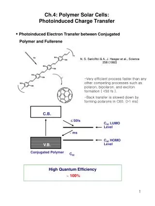
Physics on Bulk HeterojunctionSolar Cells (3) - - (2) (4) (1) O M e Donor (5) O - EF EF Diffusion length (5~10nm) Acceptor Cathode Anode (2) (5) + + + (3) (4) P3HT PCBM (1) Light absorption for exciton generation LUMO (2) Exciton diffusion LUMO (3) Exciton transfer for hole-electron separation (4) Carrier transport towards the electrodes (5) Charge collection at the respective electrodes HOMO HOMO
1. Lc/α-1 ratio ~ 1 @ peak wavelengths • 2. Over MOST of their absorption Lc/α-1 < 1, devices are thus losing great number of absorbed photons into lost carriers How do BHJSCs and DSSCs stand in terms of characteristic lengths? What can we do? Find better materials? Yes, 999,999 nerds are working on that…but… it possible to enhance optical absorption while also improving electrical performance ? Key elements: Lc/α-1 are intrinsic, but absorption and carrier travel distances no!
Designs to Enhance Light Absorption Ray Optics 1 mm θ Wave Optics 50% increase in Jsc 1 μm Kim et al., Adv. Mater. (2006). Tvingstedt et al., Appl. Phys. Lett. (2007).
Wave Optics Approach via Periodic Nanostructures Complex Nanostructures L = 1200 nm 80 nm 60 nm 5 nm 150 X enhancement compared to 4n2 for randomly roughened surface 1.8 μm Diffraction Grating Natural Inspiration Absorption enhancement Na et al., Adv. Funct. Mater. (2008). Yu et al., Proc. Natl. Acad. Sci. (2010). Tikhodeev et al., Phys. Rev. B (2002).
A Look at Nature 1.8 μm Vikusic et al.
Resonant Mode Excitations n1 = 1.8 + 0.015i n2 (pillars) = 2.5 • Absorption in increased even with reduction in volume of absorbing material • Absorption spikes depend on physical dimensions, so desired region of solar spectrum can be targeted (e.g. near band edge)
Absorption Enhancement Prediction Planar 2-D periodic 1-D periodic 2-D periodic 1-D periodic 17% increase 13% increase key J.R. Tumbleston et al., Appl. Phys. Lett. (2009).
Optical Optimization Planar 2-D periodic 1-D periodic nc-ZnO index of refraction J.R. Tumbleston et al., Opt. Express (2009).
Detailed Optical Model local absorption profile important Nanostructure Flash J.R. Tumbleston et al., Opt. Express (2009).
The chosen pattern Blend Top View 400 nm ZnO nc 220 nm 175 nm post height 22% increase in absorption
Photonic Crystal Solar Cell Fabrication Pressure + Heat Spin coat nc-ZnO Aluminum PFPE mold Si master Polymer blend PEDOT:PSS ITO Glass substrate same substrate Polymer blend Nano Lett. (2009). J. Phys. Chem. C (2010).
Robust Material: TDPTD • Nanopatterning over large area • Photonic crystal and planar cells fabricated on same substrate • Nanopattern periodicity on order of wavelength of light (400 nm) • Refractive index contrast between BHJ and nc-ZnO Nano Lett. (2009).
Encouraging Results for TDPTD:PCBM Nano Lett. (2009).
Angular Dependence of IPCE and Optical Properties s-pol p-pol θ = 15°
P3HT:PCBM Planar cell Photoactive layer (Planar) PC cell Nano-pattern layer Flash layer
The good news and the so-so news Nanofabrication optimization
What about electrical processes? 400 nm long short E-field e-/h+ e-/h+ e-/h+ e-/h+ e-/h+ e-/h+ e-/h+ e-/h+ e-/h+ e-/h+ e-/h+ e-/h+ e-/h+ We wanted a steady-state measurement of carrier transport for functional devices using photoexcited carriers that are extracted from device. • Well understood and well modeled optical enhancements • Very nice nanopatterning technique What effect does pattern have on charge creation and transport? carrier density e-/h+ Distance from Anode
single device θ = 0° λ = 473 nm Light E-field h+ e- 100 nm → 10 nm 225 nm Light From ITO – “electron restricted” From Al – “hole restricted” J.R. Tumbleston et al., Phys. Rev. B (2010).
θ = 0° λ = 473 nm Light 100 nm → 10 nm 90, 225 nm Light 90 nm active layer 225 nm active layer
Summary Photonic cell Light absorption enhancement nanofabrication, instrumentation, device characterization 1. Opt. Express 17, 7670 (2009). 2. Appl. Phys. Lett. 94, 043305 (2009). 3.Nano Lett. 9, 2742 (2009). 4. J. Phys. Chem. C (2011). 5. Soft Matter (2011). 6.Phys. Rev. B 82, 205325 (2010). 7. J. Appl. Phys. 108, 084514 (2010). 8. J. Appl Phys. 108, 083101 (2010). electro-optical measurements, transport lengths in active cells
Working towards model of PC device performance Cathode Cathode Oxide Oxide Height (m) Log (E-field) P3HT:PCBM P3HT:PCBM Anode Anode Lateral distance (m) Lateral distance (m)
Toward the actual butterfly structure Array if Silicon oxide/ Silicon nitride xmas trees Forest of Silicon pine trees
Acknowledgments: Lopez group And last but certainly no least: the current sponsors of the Lopez lab projects: Students: John tumbleston (patterned organic PV) Kristen Alexander (gold SERS) Emily Ray (metamaterials work) Yingchi Liu (Cu2O-ZnO work) Rudresh Ghosh (Naobia DSSCs) Posdocs: Mukti Aryal Abay Dinku Currently looking for more good people, ask me ! Main collaborators Doo-Hyun Ko from Ed Samulski’s group Meredith Hampton from Joe Desimone group Kyle Brenneman from Tom Meyer group Christoph Kirsh from Sorin Mitran group