Download
1 / 17
170 likes | 357 Vues
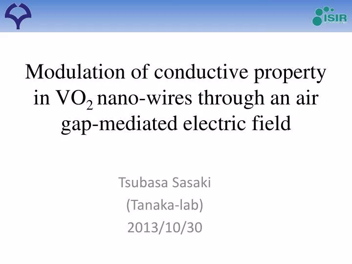
Modulation of conductive property in VO 2 nano -wires through an air gap-mediated electric field. Tsubasa Sasaki (Tanaka-lab) 2013/10/30. Contents. ・ Background Metal-insulator transition(MIT) of strongly-correlated electron(Mott) materials (ex. VO 2 )

E N D
Modulation of conductive property in VO2 nano-wires through an air gap-mediated electric field Tsubasa Sasaki (Tanaka-lab) 2013/10/30
Contents ・Background Metal-insulator transition(MIT) of strongly-correlated electron(Mott) materials (ex. VO2) Electric control of Mott transition Previous reports ・Purpose of my research W side gate FET ・Principle PLD , Nanoimprint ・Fabrication ・Experimental result Atomosphere dependence Chemical equation expected Laser Raman spectroscopy etc ・Summary
Background Strongly-correlated electron materialsVO2 Metal-insulator transition New electronic devices ex)MottFET・・・ Electron phase transition is controlled by a gate terminal. Stimulation Temperature Electric field Magnetic field Light Metal Insulator
Electric control of Mott transition By applying an electric field, VG ・Charge injection effect ・Redoxeffect H+ O2- Gate Metal Insulator Source Drain Upper Hubbard Band Insulating layer EF EF EF U Drain current Lower Hubbard Band
Previous reports M. Nakano et al, Nature 487,459 (2012) J. Jeonget al, Science 339,1402 (2013) This time, I have found what using Redox effect. Features of the transition metal oxide transistors Charge injection effect (Mott-transistor) Redox effect (Redox-transistor: development of two-terminal ReRAM)
Purpose W side gate type FET structure Electric field effect simulation ( Cross-sectional view ) イオンマイグレーション イオンマイグレーション Channel Gate Gate 電子相転移雪崩 電子相転移雪崩 Al2O3 sub. Advantage Vacuum The physical-properties measurement which combined the probe microscope etc. is possible. Measurement by various gas environment is possible.
Pulse laser depositon(PLD) 基板 V2O5焼結体 Pulse laser deposition (PLD) Production of thin film ArF(λ=193nm) レーザ VO2 Al2O3 レーザ 基板
Nanoimprint Production of structure A optical micrograph 0.5mm 4mm 4mm
Fabrication VO2 PLD(Thin films of VO2) Drain d Gate L Nanoimprint(Pattern formation of VO2) W Pt Gate Source RIE(Etching) VO2 channel A Photolithography (Electrode pattern formation) Sputtering (Pt electrode) Drain Gate Gate Source
Atmosphere dependence Air I tried to apply a gate voltage under various atmosphere (Air, N2 and Dry Air) Humidity :56% N2 Large resistance change was observed only under the air Dry Air Gradual resistance change The factor is adsorbed water(H2O) Memory effect
Chemical equation expected Cathode : (陰極) ● ● Decrease of resistivity Anode : (陽極) ● ● View of image O O O H H H H H H O O O O + - H H H H HxVO2 V2O4+x/2 Gate (Anode) Chanel (Cathode) + - + - e + + - + H + - H + + + - + H + - H O H e Al2O3 H
VO2 resistivity change in the air Air Mapping
gate-channel current The difference of gate-channel current Air The amount of current flowing along the water which is adsorbed N2 The amount of movement of the H+by electrolysis
Laser Raman spectroscopy Jiang Weiet al. Nature Nanotech 70, 357 (2012) Peak area of 600 cm-1 near Annealed in a hydrogen atmosphere Hydrogenated channel channel gate gate gate gate Peak of 199cm-1, 225cm-1, 618cm-1 decreased I believed that this is hydrogenated Hydrogen ions are diffused over the entire channel width(3μm)
Large resistance change by hydrogen doped Metal Insulator Upper Hubbard Band EF EF EF U Lower Hubbard Band
Summary Summary I was fabricated W side gate type FET structure ● Large resistance change was observed only in the air ⇒The factor is adsorbed water (H2O) ⇒Hydrogenation of VO2 by the gate electric field ● ⇒Redox-controlled Mott transistor 水の電気分解より化学反応式を立てた ● Future plan 閾値電圧が存在することが観察された ● Future work ゲート-チャネル間の電流からH+の移動 I will perform the SIMS measurement to confirm hydrogen existence in the VO2 channel ● ● SIMSの測定を行い、水素の存在を確認 ● ラマン分光より水素化によるピークの減少 ● 閾値電圧の値について、詳細に解析する ●