Download
1 / 50
640 likes | 1.08k Vues
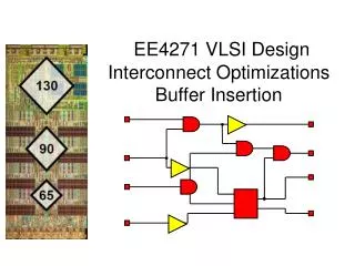
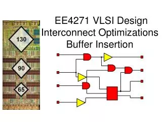
EE4271 VLSI Design Interconnect Optimizations Buffer Insertion. Moore’s law. Twice the number of transistors, approximately every two years, so double clock frequency accordingly. Interconnects Dominate. 300. 250. Interconnect delay. 200. 150. Delay (psec). 100. Transistor/Gate delay.

E N D
EE4271 VLSI DesignInterconnect Optimizations Buffer Insertion
Moore’s law Twice the number of transistors, approximately every two years, so double clock frequency accordingly
Interconnects Dominate 300 250 Interconnect delay 200 150 Delay (psec) 100 Transistor/Gate delay 50 0 0.25 0.8 0.5 0.35 0.25 0.18 0.15 Technology generation (m) Source: Gordon Moore, Chairman Emeritus, Intel Corp. This is why Moore’s law is not true anymore. 3
Objectives • What have we learned? • Compute circuit delay on wires and gates • Gate delay optimization • What are we going to learn? • Interconnect delay optimization: buffer insertion • Why reducing delay • How to perform it • This is the most important optimization in circuit design
Why is this trend? 300 250 Interconnect delay 200 150 Delay (psec) 100 Transistor/Gate delay 50 0 0.25 0.8 0.5 0.35 0.25 0.18 0.15 Technology generation (m) Source: Gordon Moore, Chairman Emeritus, Intel Corp. 5
G S D w S h l hs ls Ss ws A scaling primer • Ideal process scaling: • Device geometries shrink by S (= 0.7x) • Device delay shrinks by s • Wire geometries shrink by s • Unit resistance R/m: r/(ws.hs) = r/s2 • Unit coupling capacitance Cc/m : (hs)/(Ss) • Resistance doubled, capacitance roughly unchanged for unit length • How about the change in wire length?
Technology scaling • Global (long) interconnect lengths don’t shrink • Global interconnect link cells far apart • Local (short) interconnect lengths shrink by s • Local interconnects link cells nearby
Interconnect delay scaling • Delay of a wire of length l : tint= (rl)(cl) = rcl2 (a quadratic function of length) • Local interconnects : tint : (r/s2)(c)(ls)2 = rcl2 • Local interconnect delay unchanged • Global interconnects : tint : (r/s2)(c)(l)2 = (rcl2)/s2 • Global interconnect delay doubled – unsustainable! • Interconnect delay increasingly more dominant
Elmore Delay for Wire x unit wire capacitance c unit wire resistance r C
Elmore Delay for Buffer v u C Driving resistance Input capacitance
Elmore Delay for A Circuit • Delay = all Ri all Cj downstream from Ri Ri*Cj • Elmore delay to n1 R(B)*(C1+C2) • Elmore delay to n2 R(B)*(C1+C2)+R(w)*C2 n1 n2 R(B) B R(w) C1 C2
Buffers Reduce Wire Delay x/2 x/2 R C rx/2 R rx/2 cx/4 cx/4 cx/4 cx/4 C ∆t t_unbuf = R( cx + C ) + rx( cx/2 + C ) t_buf = 2R( cx/2 + C) + rx( cx/4 + C) t_buf – t_unbuf = RC – rcx2/4 x
l l1 l2 l3 ln Buffered global interconnects: Intuition Interconnect delay = r.c.l2/2 Interconnect delay = r.c.li2 /2< r.c.l2/2(where l = S lj ) sinceS (lj 2) < (S lj )2 (Of course, we need to consider buffer delay as well)
… … L Rd – On resistance of inverter Cg – Gate input capacitance r,c – unit resistance and capacitance l Optimal Buffer Insertion on A Wire • Delay before buffer insertion = rcL2/2 • Assume N identical buffers with equal inter-buffer length l(L = Nl) • For minimum delay,
Optimal interconnect delay • Substituting lopt back into the interconnect delay expression: Delay grows linearly with L (instead of quadratically)
80 clk-buf 70 buf 60 tot-buf 50 40 % cells used to buffer nets 30 20 10 0 90nm 65nm 45nm 32nm Total buffer count • Ever-increasing fractions of total cell count will be buffers • 70% in 32nm • 25% is widely observed
Feature size (nm) Relative 250 180 130 90 65 45 32 delay 100 Gate delay Local interconnect (M1,2) Global interconnect with repeaters Global interconnect without repeaters 10 1 Source: ITRS, 2003 0.1 ITRS projections
Exercise 1 • Given a wire of length 10 with r=2, c=2, what is its delay? • Given a buffer with Rd =10, Cg=20, after optimally buffering the wire, what is the delay? • What if wire length is 100? • Any conclusion?
Exercise 2 • Relationship with gate sizing • If we can size the buffer, what is the best buffer size? • Let R0 denote the unit size buffer driving resistance, and C0 denote the unit size buffer input capacitance. Thus, Rd=R0/h and Cg=C0h • What is best h leading to smallest delay?
Analogy • Advancing technology = period of city expansion, more transistors = larger city • Interconnects = streets • Buffers = gas stations • Signal delay (timing) = time to cross the city • Buffer insertion = gas station construction
Previous Result is Only Theoretical: Discrete Buffer Locations Candidate buffer locations
RAT: Required Arrival Time RAT = 100 AT = 0 RAT = 100 AT = 0 Wire delay = 80 Wire delay = 80 AT = 80 RAT = 20
Slack: RAT - AT RAT = 100 AT = 0 Wire delay = 80 AT = 80 RAT = 20 Slack = 20 Slack = 20 Minimizing circuit delay = maximizing RAT at driver = maximizing slack at driver
Motivation for Problem Formulation RAT = 300 AT = 350 Slack = RAT-AT= -50 slack = -50 RAT = 700 AT = 600 Slack = 100 RAT = Required Arrival Time Slack = RAT - AT RAT = 300 AT = 250 Slack = 50 Decouple capacitive load from critical path slack= 50 RAT = 700 AT = 400 Slack = 300 We need to maximum slack or RAT at driver
Timing Driven Buffering Problem Formulation • Given • A Steiner tree • RAT at each sink • A buffer type • RC parameters • Candidate buffer locations • Find buffer insertion solution such that the slack (or RAT) at the driver is maximized
An Example for Buffer Insertion C Q • r = 1, c = 1 • Rb = 1, Cb = 1 • Rd = 1 2 2 (v1, 1, 20) Add wire (v2, 3, 16) (v2, 1, 13) v1 v1 Insert buffer Add wire Add wire (v3, 5, 8) (v3, 3, 9) v1 v1 slack = 3 slack = 6 Add driver Add driver
Candidate Buffering Solution • Definition • Each candidate solution is associated with • vi: a node • ci: downstream capacitance • qi: RAT vi is a sink ciis sink capacitance vis an internal node
Van Ginneken’s Algorithm Candidate solutions are propagated toward the source
Solution Propagation: Add Wire • c2 = c1 + cx • q2 = q1 – rcx2/2 – rxc1 • r: wire resistance per unit length • c: wire capacitance per unit length x (v1, c1, q1) (v2, c2, q2)
Solution Propagation: Insert Buffer (v1, c1, q1) (v1, c1b, q1b) • c1b = Cb • q1b = q1 – Rbc1 • Cb: buffer capacitance • Rb: buffer resistance
Solution Propagation: Add Driver (v0, c0, q0) (v0, c0d, q0d) • q0d = q0 – Rdc0 • Rd: driver resistance • Pick solution with max slack
Exercise (20,400) 2 2 2 Unit Wire Cap = 5 Unit Wire Res = 3 Buffer C=5, R=1 Perform buffer insertion to maximize the slack at driver
Exponential Runtime 2 solutions 4 solutions 8 solutions 16 solutions n candidate buffer locations lead to 2n solutions
Solution Pruning • Two candidate solutions • (v, c1, q1) • (v, c2, q2) • Solution 1 is inferior if • c1 > c2 : larger load • and q1 < q2 : tighter timing
An Analogy - I Faster -> Smaller Delay -> Larger RAT (since RAT = RAToutput - Delay) Larger Load -> Larger Capacitance LOAD
An Analogy - II Faster & smaller load (larger RAT, smaller capacitance): Good END LOAD Slower & larger load (smaller RAT, larger capacitance): Inferior LOAD
An Analogy - III END Who will be the winner? Cannot tell at this moment, so keep both of them.
An Analogy - IV END Who will be the winner? Cannot tell at this moment, so keep both of them.
Pruning When Insert Buffer They have the same load cap Cb, only the one with max q is kept
(1) (2) (3) Generating Candidates From Dr. Charles Alpert
(3) (b) (a) Both (a) and (b) “look” the same to the source. Throw out the one with the worse slack (4) Pruning Candidates
(4) (5) Candidate Example Continued
(5) At driver, compute which candidate maximizes slack. Result is optimal. Candidate Example Continued After pruning
Example 2 2 2 Unit Wire Cap = 5 Unit Wire Res = 3 Buffer C=5, R=1 (20,400) (30,250) (5, 220) (20,400) (30,250) (5, 220) (40, 40) (5, 0) (15,160) (5, 145) (20,400)
Example Cont’d (30,250) (5, 220) (40, 40) (5, 0) (15,160) (5, 145) (20,400) (5,0) is inferior to (5,145). (45,40) is inferior to (15,160) (30,250) (5, 220) (15,160) (5, 145) (5,15) (5,70) (20,400) Pick solution with largest slack, follow arrows to get solution
Exercise • Without pruning, there will be exponential number of candidate solutions (i.e., given n candidate buffer locations, there will be 2n solutions). With pruning, how many solutions will we have?
Exercise • Continue the following buffer insertion process. Assume that all partial candidate buffering solutions are as shown. 2 2 (10,40) (8,50) (5,10) (15,40) (7,10) (9,30) (12,20) Unit Wire Cap = 1 Unit Wire Res = 1 Buffer C=1, R=1
Summary • Interconnect delay increases with technology scaling • Linear interconnect delay with buffer insertion • Buffer insertion with candidate buffer locations • Pruning for accelerating buffer insertion technique