Download
1 / 21
210 likes | 313 Vues
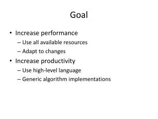
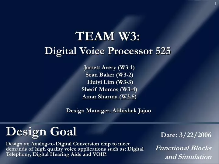
TEAM W3: Digital Voice Processor 525. Jarrett Avery (W3-1) Sean Baker (W3-2) Huiyi Lim (W3-3) Sherif Morcos (W3-4) Amar Sharma (W3-5). Design Manager: Abhishek Jajoo. Design Goal. Date: 3/22/2006 Functional Blocks and Simulation.

E N D
TEAM W3:Digital Voice Processor 525 Jarrett Avery (W3-1) Sean Baker (W3-2) Huiyi Lim (W3-3) Sherif Morcos (W3-4) Amar Sharma (W3-5) Design Manager: Abhishek Jajoo Design Goal Date: 3/22/2006 Functional Blocks and Simulation Design an Analog-to-Digital Conversion chip to meet demands of high quality voice applications such as: Digital Telephony, Digital Hearing Aids and VOIP.
Status • Design Proposal • Project chosen: 16 bit Delta-Sigma ADC • Basic specs defined • Architecture • Matlab Simulated • Behavioral Verilog - Simulated • Structural Verilog – Simulated • Schematic • Digital – All modules created • Analog - All modules created • Floorplan • Revised for signal routing • Layout • Op Amps – DRC, LVS, Simulated • Low Pass Filter – DRC, LVS, Simulated • PII – DRC, LVS, Simulated • Sinc Filter – DRC, Not LVS, Not Simulated • Simulation / Verification • All modules verified separately at transistor level and some layouts
Analog Progress • Everything is in Transistor Level and Verified • Layouts and Extracted Views of the Operational Amplifiers • Integrator - Verified • Comparator – Verified • Reviewed Common Centroid Style of Layout • More in-depth next week…
Design Decisions • Metal Directionality • Buffering – Clock to Minimize Glitching • Overall Chip Routing and Signal Directionality • Compacted Mirror-adder and DFF • Reviewed Common Centroid Layout – Next Week…
Timing and Power Total = 6,432 transistors, 509.8 uW of power
Problems and Questions • Layout is very time consuming • More metal layers or larger layouts? • Sand in my laptop
What's Next… • LVS all blocks • Sinc Filter • Analog Components • Global Routing • Wire Decimation filter and Modulator • Wire Overall Chip • Overall Chip Simulation • Extract and simulate in a mixed signal env. • Optimization