Download
1 / 71
740 likes | 1.01k Vues
Chapter 4. control unit. Agenda. Basic concepts Fundamentals of CU Register transfer notations and descriptions Buses Design methods Hardwired approach Microprogramming. Model of Control Unit. Functions of Control Unit using Control Signals. Sequencing

E N D
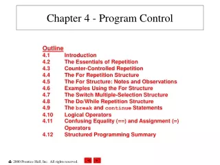
Agenda • Basic concepts • Fundamentals of CU • Register transfer notations and descriptions • Buses • Design methods • Hardwired approach • Microprogramming
Functions of Control Unit using Control Signals • Sequencing • CU causes the CPU to step through a series of micro-operations in proper sequence based on the program being executed • Execution • CU causes each micro-operation to be performed • Control Signals • External: inputs indicating the state of the system • Internal: logic required to perform the sequencing and execution functions
Fundamental Concepts • Processor fetches one instruction at a time and perform the operation specified. • Instructions are fetched from successive memory locations until a branch or a jump instruction is encountered. • Processor keeps track of the address of the memory location containing the next instruction to be fetched using Program Counter (PC). • Instruction Register (IR)
Fundamental Concepts contd.. • Purpose of control unit is to control the system operations by routing the selected data items to the selected processing HW at right time • Control unit’s responsibility is to drive the associated processing HW by generating a set of signals that are synchronized with the master clock • In order to carry out a task such as ADD, the control unit must generate a set of control signals in a predefined sequence governed by the HW structure of the processing section.
Fundamental Concepts contd.. • Inputs to control unit are: • Master clock • Status info from processing section • Command signals from external agent • Outputs produced by control unit • Signals that drive the processing section and responses to an external envt (operation complete or abort) due to exceptions (overflow and underflow) • Control unit undertakes the following responsibilities • Instruction interpretation: ( read instr. , recognize, get operands and route to appropriate functional units, necessary control signals issued) • Instruction sequencing: control unit determines the address of next instruction to be executed and loads to PC
Register transfer notations • Basis for CU design are register transfer operations Declaring registers: A[8], B[8], PC[16] Assigning registers BA Assigning higher order byte of 16 bit PC PCHI[8]= PC[15-8] Assigning individual bits A[4]=B[5] Info transfer b/w 2 registers is controlled by enable signal E(control input), driven by control unit
HW implementation of C0:AB IF A>B and D[0]=0 then AB
HW implementation If x=0 and t=1, then AB else AD
Register transfer description • DA’ • D AVB (A OR B, store result in D) • D AɅB ( A AND B, store result in D) • LSR(A) • ASR(A) • LSL, ASL, ROR, ROL • A$Q – used to concatenate A and Q • ASR(A$Q)
RWM(Read Write Memory Unit) • MBR and MAR are associated with RWM • R: MBR M((MAR)) • W: M((MAR)) MBR • The line b/w RWM and MBR is bidirectional bus and it can be easily implemented using tristate buffers
Buses • Route data in and out of a digital system • Normally 2 buses: inbus and outbus • Notations • Inbus[4] and outbus[4] -- 4 bit buses • A=inbus ( data of inbus is transferred into A register when next clock arrives • Outbus = B[7:4] ( higher order 4 bits of an 8 bit register is made available on the outbus for one clock period) Register Transfer instructions for multiplying( single bus ) Declare Registers A[8], M[8],Q[8]; Declare buses inbus[8] and outbus[8]; start: A0, Minbus; Q inbus; Loop: AA+M, Q Q-1; if Q>0 then goto loop; Outbus = A; goto halt (stop)
Buses contd… HW required • 8 bit inbus, outbus, 8 bit parallel adder, 3 8 bit registers Concurrent operations • A 0, M inbus • A A+M, Q Q-1 M inbus and Q inbus must be done serially Microoperations: operations (such as A0, AA+M) that can be done in one cycle Rate at which computer performs operations (such as A A+M, AAɅB ) is determined by bus structure Single bus structure is the simplest and cheapest
Single bus features • At any given time, data may be transferred b/w 2 CPU registers or b/w a register and ALU • Bus must be multiplexed across various operands • ALU must have buffer registers to hold transferred operand • Ex: R2 R1+R0 is completed in 3 clock cycles( 3 control states) • 1st : R1 A • 2nd : R0B • Sum produced by ALU is loaded into R2 , when 3rd clock pulse arrives Disadvantages: • Affects speed of execution of a typical 2 operand memory • Increases no. of states in control logic. Hence more HW may be required to design control unit
double bus contd… Features: • All general purpose registers are connected to both buses • Both operands are routed in one cycle • Special purpose registers are divided into 2 groups • Each group is connected to one of the buses • Data from 2 special purpose registers of the same group cannot be transferred to the ALU at the same time • Whenever there is a need to process simultaneously the contents of 2 special purpose registers of the same group, contents of one of the registers must be transferred to GPR prior to processing.
double bus contd… Features contd: • Output Buffer register is used to prevent collision of the buses • 1st cycle: loading operands and storing result in O/P buffer • 2nd cycle: result in O/P buffer is pushed to bus(destination) • There can be dedicated paths b/w PC and MAR
3 bus features • Addition of bus C allows to perform ALU operations such as R2 R0+R1 in one cycle • Increase system cost and control logic is complicated • There can be small delays
Timing signals • Control unit has to properly sequence a set of operations • Sequence of N consecutive operations will occur in response to N consecutive clock pulses • To carry out an operation Pi in ith clock pulse, CU must count the clock pulses and produce a timing signal Ti. • Ti will assume value of 1 during the duration of the ith clock pulse
Timing signals contd… • Timing signals are generated using a ring counter • This system will sequence the following manner
Timing signals contd… • Boolean equations for each timing variable are T0=A, T1=B, T2=C, T3=D Disadvantage: • N flip flops are required to generate N timing signals • Not economically feasible for large values of N
Overview • To execute instructions, the processor must have some means of generating the control signals needed in the proper sequence. • Two categories: hardwired control and microprogrammed control • Hardwired system can operate at high speed; but with little flexibility.
Hardwired vs Microprogrammed • Hardwired • Use gates to generate signals • Squeeze out the juice for performance(not flexible) • Different logic styles possible • Economical initially • Small changeredesign • Microprogrammed • Store the control signals in the sequence • Just read from the memory every clock cycle • Expensive initially • Additions done by simply changing the microprogram in control memory • Diagnostics routine can be made available in memory
HARDWIRED APPROACH • Final circuit is obtained by physically connecting gates and flip flops • Cost of control logic increases with system complexity
Hardwired Unit CLK IR Ring Counter T5 T1 Opcode LDA Decoder Control Matrix STA ADD SUB MBA JMP JN Halt NF Control Signals
Control Matrix • Implement using discrete gates • Usually done using PLAs • Large control matrices are implemented hierarchically • For speed • A well known process and design flows are widespread
10 steps for hardwired control • Define task to be performed • Propose a trial processing section • Provide a register transfer description of the algo based on the processing section outlined in the previous step • Validate the algo by using trial data • Describe the basic characteristics of the HW elements to be used in the processing section • Complete the design of the processing section by establishing necessary control points • Propose the block diagram of the controller • Specify state diagram of controller • Specify the characteristics of the HW elements to be used in the controller • Complete the controller design and draw a logic diagram of final circuit
Ex: booth’s multiplier to multiply 2 4-bit 2’s complement no Step 1: Task definition Design a Booth’s multiplier to multiply two 4-bit 2’s complement numbers Step 2: trial processing section q1 q0 0 0none 0 1 add M 1 0sub M 1 1 None
Contd.. Step 3: register transfer description Declare registers A[4], M[4], Q[5], L[3] Declare buses Inbus[4], outbus[4] Start: A0, Minbus, L4; clear A and transfer M Q[4:1]inbus, Q[0]0; transfer Q Loop: if Q[1:0]=01, then go to ADD; if Q[1:0]=10, then go to SUB; go to Rshift; ADD: AA+M; goto Rshift; SUB: AA-M; Rshift:ASR(AQ), LL-1; if L>0, then go to loop outbus =A; outbus=Q[4:1]; go to halt
Contd.. Step 5: functional characteristics of HW elements of processing section
Step 6 contd… • There are 10 control points • C0 held high A reg is cleared with trailing edge of next clock • 1 control point is introduced for each microoperation specified in the register transfer description • Processing section extends 3 outputs Q[1], Q[0] and Z (decision making)
state diagram contd… • There are 9 states and hence 9 non overlapping timing signals have to be generated • Mod 16 counter and a 4 to 16 decoder can be used to accomplish this task
Step 9: characteristics of HW elements used in controller Mod 16 counter
Step 10 contd…(truth table for SC) • Sequence controller sequences the controller as indicated in state diagram • Truth table for SC
Step 10 contd… • When L is 0, counter will automatically count up in response to next clock pulse. • Hence counter is a normal up counter and should change normal operation only during certain conditions. • Such normal sequencing is required • Present control state is T0,T1,T4,T6 OR T7 • Present control state is T2 and Q[1] Q[0]=01 • Present control state is T5 and Z=1 • Hence the SC must exercise control only when there is a need for the counter to deviate from its normal counting sequence
PLA for designing SC • Though SC has 8 inputs(256 combinations) , it must examine only a few possibilities • Designers use programmed logic array (PLA) in this situation
PLA contd… • For each row of SC truth table, product term is generated in PLA P0= Q[1]’ Q[0]’ T2 P1= Q[1] Q[0] T2 P2= Q[1] Q[0]’ T2 P3=T3 P4=Z’T5 P5=T8 L= P0+P1+P2+P3+P4+P5 d3= P5 d2= P0+P1+P2+P5 d1=P4 d0=P0+P1+P3