Download
1 / 14
140 likes | 177 Vues
THERMAL CONDUCTIVITY OF SILICATE BONDED SAMPLES. Status of measurements with the thermal conductivity facility in Firenze. October, 8 th 2007. Gianpietro Cagnoli a,c), Enrico Campagna a,d), Elisabetta Cesarini a,b) , Matteo Lorenzini a), Giovanni Losurdo a),

E N D
THERMAL CONDUCTIVITY OF SILICATE BONDED SAMPLES Status of measurements with the thermal conductivity facility in Firenze October, 8th 2007 Gianpietro Cagnoli a,c), Enrico Campagna a,d), Elisabetta Cesarini a,b), Matteo Lorenzini a),Giovanni Losurdo a), Filippo Martelli a,d), Francesco Piergiovanni a,d), Flavio Vetrano a,d) • INFN Sez. Firenze • Dip. di Astronomia e Scienza della Spazio • University of Glasgow • Università di Urbino
FACILITIES IN FIRENZE LAB THERMAL NOISE • Thermal noise levels depend on several thermomechanical parameters of materials – which are interesting in general for designing, such as: • mechanical loss rate • thermal conductivity • specific heat capacity, thermal expansion • elastic constants, breaking strength… Thermal noise falls down with reducing T, so it is worth studying these parameters down to cryogenic conditions.
PROPERTIES OF SILICON Cryogenic candidate material: Silicon Low losses: (Lam and Douglas, 1981) At cryogenic temperatures: (D. F. McGuigan et al. 1978)
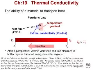
INSULATOR BOX HEATER CLAMP THERMOMETERS 30 cm SAMPLE SAMPLE HEATER COPPER BOX Pure Si L=5.8 cm, Ø=5.0 mm THERMAL CONDUCTIVITY MEASUREMENTS ON SILICON SAMPLES (K is the conductance)
THERMAL CONDUCTIVITY MEASUREMENTS ON SILICON SAMPLES Si sample: purity 10-6 r = 42 W cm (measured) Presented at GWADW VESF Meeting 2006 From Y.S. Touloukian, E.H. Buyco, “Thermo-physical properties of matter”, Plenum, NY, 1970
Si – O - Si KOH Silicate bonded samples supplied by Glasgow IGR group: it was needed a new arrangement, suitable for 1’’ bonded disks, 12 mm thick THERMAL CONDUCTIVITY MEASUREMENTS Silicate bonding is used for assembling monolithic suspensions. Does it change or spoil the silicon high conductivity?
SILICATE BONDING MEASUREMENT Sample with 1” diameter, 12 mm thick By moving to the new peculiar geometry of silicate bonded disks, several difficulties arise: • PT1000 position against the lateral surface should be known as precisely as possible, since it enters the conductibility measurement • Very high conductance requires the power flowing to be pretty high for temperature gradient to become measurable; • Thermal contacts are a determinant issue, and in general heat flux must be kept homogeneous; • Sample (bonding) inhomogeneities spoil the measurement accuracy by bending the heat path.
CURRENT SETUP PT1000 INDIUM FOILS • Indium foils inserted • Sharp blades sensing T • 2 PT1000 each sensor • Enhanced sensitivity
across Bonding Pure Si 150 W/mK 160 W/mK CURRENT SETUP With the current setup (with old copper heating coil), we obtained the first good measurement at room temperature: 1 mK (Si @ 300K has ~150 W/mK) PT1000 calibration power calibration geometry
A GOOD THERMAL CONTACT In order to have a homogenous heat flux, thermal contacts must be realized carefully. We found that the contact between sample and heater (and sink) was not good, even with grease. By inserting indium disks, contact is good all across the surface SINK HEATER
INHOMOGENEITIES IN THE BONDING LAYER If the bonding realizes a bad thermal contact in some point between the two disks, measurements can be severely altered.
INHOMOGENEITIES IN THE BONDING LAYER On the ring sensor, a 2mm lateral cut in the bonding results in 30 mK spread of T over a 1K total temperature gradient. Depending on the position of PT1000s, that leads to an error as high as 3%. Temperature on an aluminum sensor with a 2mm cut in the bonding layer (1K is set across the whole sample)
FIRST CONDUCTIVITY CURVE A first complete curve of conductivity for the third sample has been obtained: Thermal Conductivity [W/(m K)] Temperature [K]
CONCLUSIONS and FUTURE WORK • In its final version, the facility behaves well and reveals • inhomogeneities on 1” disk samples; • Going down to Helium will request new sensors (like • CERNOX, already available) and represents a major • improvement; • Samples with new requested geometry (1’’x16 cm) are • being produced in Glasgow; • Breaking strength tests correlated with conductivity • measurements.