Download
1 / 11
110 likes | 259 Vues
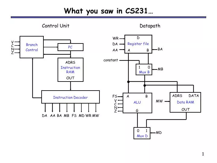
D Register file A B. WR DA AA. BA. Branch Control. V C N Z. constant. PC. 1 0 Mux B. MB. ADRS Instruction RAM OUT. ADRS DATA Data RAM OUT. FS. A B ALU G. MW. V C N Z. Instruction Decoder. DA AA BA MB FS MD WR MW. 0 1 Mux D. MD.

E N D
D Register file A B WR DA AA BA Branch Control V C N Z constant PC 1 0 Mux B MB ADRS Instruction RAM OUT ADRS DATA Data RAM OUT FS A B ALU G MW V C N Z Instruction Decoder DA AA BA MB FS MD WR MW 0 1 Mux D MD What you saw in CS231… Control Unit Datapath
0 M u x 1 Add PC 4 Add Shift left 2 PCSrc RegWrite MemToReg MemWrite Read address Instruction [31-0] I [25 - 21] Read register 1 Read data 1 ALU Read address Read data 1 M u x 0 I [20 - 16] Zero Read register 2 Instruction memory Read data 2 0 M u x 1 Result Write address 0 M u x 1 Write register Data memory Write data Registers I [15 - 11] ALUOp Write data MemRead ALUSrc RegDst I [15 - 0] Sign extend …grew up!
D Register file A B WR DA AA BA Branch Control V C N Z constant PC 1 0 Mux B MB ADRS Instruction RAM OUT ADRS DATA Data RAM OUT FS A B ALU G MW V C N Z Instruction Decoder DA AA BA MB FS MD WR MW 0 1 Mux D MD PC & branch control Control Unit Datapath
0 M u x 1 Add PC 4 Add Shift left 2 PCSrc RegWrite MemToReg MemWrite Read address Instruction [31-0] I [25 - 21] Read register 1 Read data 1 ALU Read address Read data 1 M u x 0 I [20 - 16] Zero Read register 2 Instruction memory Read data 2 0 M u x 1 Result Write address 0 M u x 1 Write register Data memory Write data Registers I [15 - 11] ALUOp Write data MemRead ALUSrc RegDst I [15 - 0] Sign extend PC & branch control
D Register file A B WR DA AA BA Branch Control V C N Z constant PC 1 0 Mux B MB ADRS Instruction RAM OUT ADRS DATA Data RAM OUT FS A B ALU G MW V C N Z Instruction Decoder DA AA BA MB FS MD WR MW 0 1 Mux D MD Instruction memory & decoding Control Unit Datapath
0 M u x 1 Add PC 4 Add Shift left 2 PCSrc RegWrite MemToReg MemWrite Read address Instruction [31-0] I [25 - 21] Read register 1 Read data 1 ALU Read address Read data 1 M u x 0 I [20 - 16] Zero Read register 2 Instruction memory Read data 2 0 M u x 1 Result Write address 0 M u x 1 Write register Data memory Write data Registers I [15 - 11] ALUOp Write data MemRead ALUSrc RegDst I [15 - 0] Sign extend Instruction memory & decoding
D Register file A B WR DA AA BA Branch Control V C N Z constant PC 1 0 Mux B MB ADRS Instruction RAM OUT ADRS DATA Data RAM OUT FS A B ALU G MW V C N Z Instruction Decoder DA AA BA MB FS MD WR MW 0 1 Mux D MD Register file Control Unit Datapath
0 M u x 1 Add PC 4 Add Shift left 2 PCSrc RegWrite MemToReg MemWrite Read address Instruction [31-0] I [25 - 21] Read register 1 Read data 1 ALU Read address Read data 1 M u x 0 I [20 - 16] Zero Read register 2 Instruction memory Read data 2 0 M u x 1 Result Write address 0 M u x 1 Write register Data memory Write data Registers I [15 - 11] ALUOp Write data MemRead ALUSrc RegDst I [15 - 0] Sign extend Register file
D Register file A B WR DA AA BA Branch Control V C N Z constant PC 1 0 Mux B MB ADRS Instruction RAM OUT ADRS DATA Data RAM OUT FS A B ALU G MW V C N Z Instruction Decoder DA AA BA MB FS MD WR MW 0 1 Mux D MD ALU & data memory Control Unit Datapath
0 M u x 1 Add PC 4 Add Shift left 2 PCSrc RegWrite MemToReg MemWrite Read address Instruction [31-0] I [25 - 21] Read register 1 Read data 1 ALU Read address Read data 1 M u x 0 I [20 - 16] Zero Read register 2 Instruction memory Read data 2 0 M u x 1 Result Write address 0 M u x 1 Write register Data memory Write data Registers I [15 - 11] ALUOp Write data MemRead ALUSrc RegDst I [15 - 0] Sign extend ALU & data memory
So what’s new? • Different ISA • Less of a “toy” example • Can see why single-cycle multi-cycle would help