Download
1 / 29
290 likes | 332 Vues
Get an in-depth understanding of system-level design with a focus on simulation-based methodology. Explore issues, models, platforms, and tools in system design, and reap benefits like productivity gains. Discover how to bridge the behavior and structural gaps for efficient system design with minimum components.

E N D
New Strategies forSystem Level Design Daniel Gajski Center for Embedded Computer Systems (CECS) University of California, Irvine gajski@uci.edu
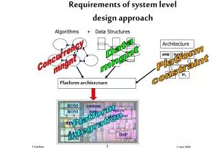
Overview • Introduction • Issues • Models • Platforms • Tools • Benefits • Conclusion
Closing the System Gap Real gap: behavior and structure (semantics and syntax)
Simulation Based Methodology Ambiguous semantics of hardware/system level languages Simuletable but not synthesizable or verifiable
In Search of a Solution Algebra: < objects, operations> Arithmetic algebra allows creation of expressions and equivalences
Model Algebra Model algebra: <objects, compositions> Model algebra allows creation of models and model equivalences
Specify-Explore-Refine Methodology Design decisions Model refinement Replacement or re-composition FPGA board
How many models? Minimal set for any methodology (3 is enough) • System specification model (application designers) • Transaction-level model (system designers) • Pin&Cycle accurate model (implementation designers)
Three Models (with Respect to OSI) Pin / Cycle Accurate Model Transaction Level Model Specification Model 7 . Application 7 . Application Spec 6 . Presentation 6 . Presentation 5 . Session 5 . Session 4 . Transport 4 . Transport 3 . Network 3 . Network 2 b . Link + Stream 2 b . Link + Stream 2 a . Media Access Ctrl 2 a . Media Access Ctrl TLM 2 a . Protocol 2 a . Protocol 1 . Physical 1 . Physical Address lines Data lines Control lines P/CAM Source: G Schirner
C1 System Specification CPU Mem • Computation • Behaviors (in C) B1 B2 v1 Communication • Channels (in C) • Variables (in C) C2 Bridge Arbiter B3 B4 HW IP System Definition = (Partial) Platform + (Partial) Spec
Transaction-Level Model (TLM) Mem CPU B1 B2 OS Drivers HAL CPU Bus IP Bus B3 B4 HW IP
Pin/Cycle Accurate Model (P/CAM) Mem Program CPU EXE IC RTOS HAL Bridge Arbiter P/CAM is downloaded automatically for fast prototyping with FPGAs or ASIC design IP HW Source: D. Gajski et al.
How many components? Minimal set for any design (4 is enough?) • Processing element (PE) • Memory • Transducer / Bridge • Arbiter
PE 2.1(Master) PE 3.1 PE 1.1 PE 1.2 Transducer1-2 PE 2.2(Slave) Memory 1 Memory 3 General System Model Arbiter 2 Arbiter 1 Interrupt2.1 Interrupt1.1 Interrupt2.2 Arbiter 3 Transducer2-3 Interrupt3.1 Interrupt3.2 Bus2 Bus1 Bus3
FSMD2<clk2> FSMD1<clk1> Memory1 Memory2 Transducer Model Addr bus1 Addr bus2 Data bus1 Data bus2 PE2 PE1 Transducer Ready1 Interrupt2 Interrupt1 Ack_ready1 Ready2 Ack_ready2 Processor1<clk1> Processor2<clk2> Data1 Data2 Queue<clk3> Source: H. Cho
Processing Element: NISC technology • Direct compilation of C to HW (fastest possible execution) • Statically and dynamically reconfigurable (anytime, anywhere) • Designed for manufacturability (solving timing closure) Programmable controller Datapath Multi-cycle units Pipelined units Controller pipelining Datapath pipelining Data forwarding
General System Design Environment Model A Estimation Refinement tool tool Synthesis Transforms: Simulation GUI Verify tool t1 tool tool t2 . . . ti tn Component library Model B
How many tools? Minimal set for any methodology (2 is enough?) • Front-End (for application developers) • Input: C, C++, Mathlab, UML, … • Output: TLM • Back-End (for SW/HW system designers) • Input : TLM • Output: Pin/Cycle accurate Verilog/VHDL
ES Environment Decision User Interface (DUI) Validation User Interface (VUI) Compiler ESE Front – End System Capture + Platform Development Create Debugger Select Stimulate Partition Verify Map TIMED Compile CYCLE ACCURATE Replace ESE Back – End Compile SW Development + HW Development Check Simulate Verify Application Tools : Compilers/Debuggers Commercial Tools : FPGA, ASIC
Does it work? • Intuitively it does • Well defined models, rules, transformations, refinements • Worked in the past: layout, logic, RTL? • System level complexity simplified • Proof of concept demonstrated • Embedded System Environment (ESE) • Automatic model generation • Model synthesis and verification • Universal IP technology (NISC) • Productivity gains greater then 1000 • Benefits • Large productivity gains • Easy design management • Easy derivatives • Shorter TTM
Design flow with NISC technology for(inti=0; i<8; i++) for(intj=0; j<8; j++){ sum=0; for(intk=0; k<8; k++) sum = sum + A[i][k] ×B[k][j]; C[i][j] = sum; } for(inti=0; i<8; i++) for(intj=0; j<8; j++){ i8 = i × 8; sum = *(A + i8) × *(B + j); sum += *(A + i8 + 1) × *(B + 8 + j); ... C[i][j] = sum; } Code Refinement Application NISC Compiler Application NISC Compiler Results Results NISC Refinement NISC NISC Iterative design & refinement Source: M. Reshadi
Performance Power saving Energy saving Area reduction 10X 5.3X 0.83X 1.3X 2.1X 1.3X 11.6X 12.8X 0 2.1X 2.5X 3X 1.25X NA NA NA DCT with NISC technology NMIPS vs. MIPS CDCT3 vs. NMIPS CDCT7 vs. NMIPS CDCT7 vs. Manual Source: B. Gorjiara
MP3 on Xillinx with ESE • Area • % of FPGA slices and BRAMS • Performance • Time to decode 1 frame of MP3 data Source: S. Abdi
MP3 on Xillinx with ESE using NISC • Area • NISC uses fewer FPGA slices and more BRAMs than manual HW • Performance • NISC comparable to manual HW and much faster than SW
Development Time with ESE Manual Development Time • Model Development time • Includes time for C, TLM and RTL Verilog coding and debugging • ESE drastically cuts RTL and Board development time ESE Source: S. Abdi
X 18.06 hrs 17.71 hrs 17.56 hrs hours 15.93 hrs Validation Time Validation Time with ESE • Simulation time measured on 3.3 GHz processor • Emulation time measured on board with Timer • ESE cuts validation time from hours to seconds ESE Source: S. Abdi
Conclusions • Extreme makeover is necessary for a new paradigm, where • SW = HW = SOC = Embedded Systems • Simulation based flow is not acceptable • Design methodology is based on scientific principles • Model algebra is enabling technology for • System design, modeling and simulation • System synthesis, verification, and test • What is next? • Change of mind • Application oriented EDA • Looking for early adapters
Thank You Daniel Gajski Center for Embedded Computer Systems (CECS) www.cecs.uci.edu