Download
1 / 74
1.08k likes | 1.96k Vues
Switched Capacitor Filters. Plan. Lecture1: Integration Techniques Switched capacitor theory Parasitic effects in switched capacitor integrators Lecture2: Switched capacitor noise Continuous time domain to sampled domain mapping Synthesis methods. Pole Requirements for stable systems.

E N D
Plan Lecture1: • Integration Techniques • Switched capacitor theory • Parasitic effects in switched capacitor integrators Lecture2: • Switched capacitor noise • Continuous time domain to sampled domain mapping • Synthesis methods
Pole Requirements for stable systems Laplace Transform: F(s) = f(t) est dt 0 From Inverse Laplace Transform all poles, si = i+ jwi of form 1/(s- i) , 1/((s – i) 2+bi2),etc contain factor: e iT for i >=0 Z-Transform: F(z) = f(nT) z -n where z = esT n=0 From Inverse Z-Transform all poles, Zi = ai + jbi of form 1/(Z-aT) , 1/(Z – aT) 2, contain factor: anT = | Zi | n in the transient response for | Zi |>1 S-Plane Z-Plane jb jw a For a stable continuous-time system All poles, si must be in LHP (i <= 0) Transfer Function cannot have poles with positive real parts For a stable sampled system All poles, Zi must obey | Zi | < 1 Objective: Map a Continuous-Time (C.T.) domain (analog) filter transfer function(T.F.), Ha(Sa) to a Discrete-Time (D.T) domain transfer function, H(z) by replacing Sa by some function Sa = f(z) Ha(Sa) H(z) with Sa = f(z) Question: What are requirements of f(z) to be a “good” mapping?
Requirements for “good” mapping function f(z) • Ha(Sa) H(z) • with Sa = f(z) • e.g., Continuous Time Integrator • Ha(sa) = 1/sRC • Requirements for f(z): • f(z) is a rational function of z, i.e.,a division of two polynomial functions • For s = jw, |Z|=1 must be true • For Re(s) < 0, |Z|<1 must be true
Integration Techniques1 (Forward Euler Example) For a C.T.filter with T.F. =Ha(Sa), it’s response can be determined from it’s state equations, a system of 1st order equations which describe it. Where: xi are the state variables of the filter gi (t) are linear functions of xi (t) and the input signal And we assume xi (t) = 0 for t <= 0 …Eq.1 …Eq.2 Now derive the state equations for sampled data systems: Integrating Eq.1 over the nth sampling period: gi(t) Forward Euler nT-T nT Now Eq.1 has been transformed into difference form. Numerical Integration can be used to evaluate this integral: e.g., for the Forward Euler approximation
Integration Techniques2 In the same way, different numerical Integration techniques will give different approximations of gi(t)dt and each will yield a different function f(Z) for transforming from Continuous-time to Discrete-Time domains. • nT nT • gi(t)dt = dxi(t)/dt.dt = xi(nT) - xi(nT-T) • nT-T nT-T • f(z). Xi(z) = Gi(z) for some function f(z) Integration Technique: xi(nT) - xi(nT-T) =Xi(z) – z –1 Xi(z)= Solve for f(z)= Gi(z)/Xi(z) Tgi(nT-T) T.z –1 .Gi(z) Tgi(nT) T.Gi(z) (T/2)(gi(nT-T) +gi(nT)) (T/2)(z –1 .Gi(z)+ Gi(z)) (Not used because unstable in Z-domain) gi(t) a) Forward Euler nT-T nT b) Backward Euler nT-T nT c) Trapezoidal/ Bilinear nT-T nT d) Mid-point nT-T nT
Integration Techniques3 • Check Mapping properties of f(z) vs Requirements • e.g., For Forward Euler Mapping: • F(Z) is a Rational Function of Z? Yes. • Let sa = ja => ja = (Z-1)/T • => z = ja T + 1 • But |z| = 1 only at a = 0 • |z| ~= 1 at a T << 1, I.e., when fs = 1/T >> a Z-Plane jb a 1 Image of j axis H(j a ) From how F(Z) functions map poles and zeros from C.T. to D.T. domains we can see: Continuous-Time Filter Dominant poles (I.e., closest to j axis in s-plane) move towards |Z|=1. (To see this let a0) => Results in peaking in passband H(ejwT) Sampled-Time Filter (Forward Euler) In Forward Euler Zero’s on jw axis are not mapped onto |Z|=1. So no zero’s in Discrete-Time T.F. => Deteriorated stopband response In Backward Euler, dominant poles move away from |Z|=1 => Results in rounding in passband H(ejwT) Sampled-Time Filter (Backward Euler) In Backward Euler, Zero’s on jw axis not mapped to |Z|=1 => Deteriorated stopband response
Switched Capacitor Theory • Resistor & equivalent switched capacitor. • Interest of switched capacitors in IC. • Basic structures of switched capacitor integrators. • Comparison with continuous time integrator.
VA VB VA VB 1 C 1 2 2 Tc Principle(Parallel mode) R
VA VB 1 C 1 2 2 Principle(Serial mode) R VA VB Tc
Interest of switched capacitors • Pole accuracy: • Tolerance on integrated resistor (σR) 20% to 30% • Tolerance on integrated capacitor (σC) 10% to 20% Accuracy on RC poles around 50% (Or more likely σRC = (σR2+σC2)0.5 = 0.36 ) • Tolerance on integrated capacitor matching 0.1% • Tolerance on clock frequency few ppm • Accuracy on SC poles better than 1% • Components size • High resistance value : PREVIOUSLY BIG RESISTOR SMALL (Switched) CAPACITOR
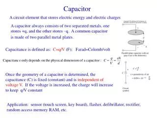
CI - + R VIN VOUT - + Continuous Time Integrator 4/Continuous Time Integrator Transfer function:
Switched Capacitor Integration Techniques We will establish on the following pages: Correspondance Table Summary Parallel Switched-Capacitor Integrator Forward Euler Mapping Serial Switched-Capacitor Integrator Backward Euler Mapping Serial/Parallel Switched-Capacitor Integrator Bilinear Mapping
CI - + 1 For (Q)=0 at node X Final-Initial VIN 1 2 2 At +Node of Capacitors VOUT + CU - - + Switched Capacitor Integrator 1/ Parallel Integrator Sampling Instant VIN X a) Calculate Transfer Function: b) Relate S.D. T.F. to Integration model: This is equivalent to Forward Euler integration
Switched Capacitor Integrator 1 For (Q)=0 at node X Final-Initial 1 2 2 At +Node of Capacitors - + 2/ Serial Integrator Sampling Instant CI VIN - + CU X - + VIN VOUT a) Calculate Transfer Function: b) Relate C.T. T.F. to Integration model: Equivalent to Backward Euler Integration
Switched Capacitor Integrator CI - + 1 CU1 - + For (Q)=0 at node X Final-Initial 1 2 2 At +Node of Capacitors VOUT + CU2 - - + 3/ Parallel/Serial Integrator Sampling Instant VIN VIN X b) Relate C.T. T.F. to Integration model: a) Calculate Transfer Function: 2 + - Equivalent to Bilinear Integration Notice: For same RC pole Cu1=Cu2=Cu/2 of previous serial or parallel integrators
35 30 25 20 15 Gain(dB) 10 5 0 -5 -10 -15 0 0.2 0.4 0.6 0.8 1 1.2 1.4 1.6 1.8 2 -80 RC integrator Parallel SC integrator -85 Phase(deg) -90 -95 -100 0 0.2 0.4 0.6 0.8 1 1.2 1.4 1.6 1.8 2 Frequency Comparison of parallel and C.T. Integrators Sample Domain Frequency,w (normalised to w0)
Comparison of serial and C.T. Integrators 35 30 25 20 15 Gain(dB) 10 5 0 -5 -10 -15 0 0.2 0.4 0.6 0.8 1 1.2 1.4 1.6 1.8 2 -80 RC integrator Serial SC integrator -85 Phase(deg) -90 -95 -100 0 0.2 0.4 0.6 0.8 1 1.2 1.4 1.6 1.8 2 Frequency
35 30 25 20 15 Gain(dB) 10 5 0 -5 -10 -15 0 0.2 0.4 0.6 0.8 1 1.2 1.4 1.6 1.8 2 -80 RC integrator Parallel/Serial SC integrator -85 i.e.,BILINEAR TRANSFORM Phase(deg) -90 -95 -100 0 0.2 0.4 0.6 0.8 1 1.2 1.4 1.6 1.8 2 Frequency Comparison with parallel/serial integrator
Parasitic effects in SC integrators • Clock overlap • Parasitic capacitors • Switch resistance • Clock feed through • Charge injection • Mismatch
CI - + - + 1 2 1 2 VIN + + CU CU - - - - - + + + Sampling Instant VIN - + 2 1 1 VIN + 2 CU - Need of non overlapping clocks CI VIN VOUT VOUT CI VOUT
Non overlapping clocks generator D1 CK CK1P D1 CK1N CK CK1P D2 CK2P CK1N CK2N D2 D1 CK2N D2 CK2P
Sampling Instant CI VIN - + VIN VOUT + 1 CU - Cp2 Cp1 2 1 2 - + Parasitic Capacitors (Parallel Integrator) X THIS TYPE OF INTEGRATOR IS SENSITIVE TO PARASITIC CAPACITORS ( INTERCONNECT, JUNCTIONS) POLE ACCURACY IS NO LONGER TRUE
Cp2 Cp1 CI Sampling Instant + VIN + - + + 1 Cu 2 1 2 1 2 - + Structure insensitive to parasitic capacitor (Equivalent Parallel Integrator) X VIN VOUT NON-INVERTING INTEGRATOR SAME TRANSFER FUNCTION AS PARALLEL INTEGRATOR EXCEPT THE SIGN POLE ACCURACY IS RECOVERED
Cp2 Cp1 Sampling Instant CI + VIN + - + + 1 Cu 1 1 2 2 2 - + Structure insensitive to parasitic capacitor (Equivalent Serial Integrator) X VIN VOUT INVERTING INTEGRATOR SAME TRANSFER FUNCTION AS SERIAL INTEGRATOR POLE ACCURACY IS RECOVERED
1 C RON 2 Switch resistance After charging C for one (non-overlap) clock phase: VIN Ts i.e., RON.C pole frequency must be more than twice the sampling frequency for capacitor charging error of <0.1%:
VG C Cgs Cgd Clock Feed-Through SWITCH ON SWITCH OFF TRANSITION ON ->OFF VC VIN VG • CLOCK FEED-THROUGH INDUCES DC OFFSET BUT NO NON-LINEARITY because no dependency on VIN ICgs
VG1 VG1 VG2 C Cgd1 Cgs1 VC ICgs1 VIN W W/2 Cgd2 Cgs2 ICgs2 Clock Feed-Throughcompensation methods (1) VG2 DUMMY SWITCH ICgd2 SINGLE TYPE OF SWITCH NMOS OR PMOS TRUE IF AND
VGn VGn C Cgdn Cgsn Cgdp Cgsp ICgsp Clock Feed-Throughcompensation methods (2) VC VGp VIN ICgsn VGp COMPLEMENTARY SWITCHES NMOS AND PMOS TRUE IF AND
C C - - - - - - - - - - - - - - - - Charge Injection • When Vg=+V is applied, P-type acceptor Holes are • repelled from surface • Negative acceptor atom space charge left in depletion layer • As Vg increases, an inversion layer of electrons forms at surface • This negative charge is redistributed when Vg0 Vg=+V N+ N+ SWITCH ON Pwell Vg=0 N+ SWITCH OFF Pwell
C Charge Injection SWITCH ON SWITCH OFF VG 1- TRANSITION ON ->OFF VC VIN D DEPENDS ON THE IMPEDANCES SEEN AT VIN AND VC TERMINALS CHARGE INJECTION INDUCES NON-LINEARITY because charge injection has a dependency on VIN
1D 2 Cu Cu Cu Cu Cu Cu 1D 1D 2 2 1 2D 2D 1 2D 1 2 1D 1D 1D 2 2 2D 1 2D 1 2D 1 Charge Injectioncompensation method Towards low-impedance input CHARGE INJECTION HIZ AT Cu SIDE CLOCK NON-OVERLAP SAMPLING CHARGE INJECTION Don’t care SAMPLING RE-DISTRIBUTION
Mismatch 5 25 5 C2 C2 25 5 5 C1 5 C1 5
Noise in SC integrators • Low pass filtering • Sampling • Aliasing • Holding
RON C WHITE NOISE fc LPF SAMPLE HOLD 10 10 10 10 10*log10(s(x)*sinc(x)**2) 5 5 5 5 0 0 0 0 Gain(dB) Gain(dB) Gain(dB) Gain(dB) -5 -5 -5 -5 -10 -10 -10 -10 -15 -15 -15 -15 -20 -20 -20 -20 -4 -2 0 2 4 -4 -2 0 2 4 -4 -2 0 2 4 -4 -2 0 2 4 Frequency Frequency Frequency Frequency SAMPLING & HOLD LOW-PASS FILTERED WHITE NOISE PSD = Power Spectral Density Sampling frequency Fs=1 -3dB frequency Fp=2 PSD WHITE NOISE PSD AFTER LPF PSD AFTER SAMPLING PSD AFTER HOLD
C RON LOW-PASS FILTERED WHITE NOISE Switch model: Resistor in series with Johnson Noise source 4kTRdf RON C Total noise power is independent of RON
0 0 10*log(g(f)**2) -1 -1 -2 -2 -3 Gain(dB) -3 Gain(dB) -4 -4 -5 -5 -6 -6 -3 -2 -1 0 1 2 3 -3 -2 -1 0 1 2 3 Frequency Frequency Under-sampling factor Ondulation function 1when .fp.Ts>>1 SAMPLING LOW-PASS FILTERED WHITE NOISE 0 -2 -4 -6 Gain(dB) -8 -10 -12 -14 -3 -2 -1 0 1 2 3 Frequency PSD AFTER LPF PSD AFTER SAMPLING SAMPLING As RON decreases, PSDSAMPLED increases
10 10 gd(x) gd(x) gd_1(x) gd_1(x) gd_2(x) gd_2(x) gd_3(x) 5 gd_3(x) gd_4(x) 5 gd_4(x) gd_5(x) gd_5(x) gd1(x) gd1(x) gd2(x) gd2(x) gd3(x) 0 gd3(x) gd4(x) 0 gd4(x) gd5(x) gd5(x) 10*log10(usf(x)) 10*log10(usf(x)) -5 Gain(dB) -5 Gain(dB) -10 -10 -15 -15 -20 -20 -5 -4.5 -4 -3.5 -3 -2.5 -2 -1.5 -1 -0.5 0 0.5 1 1.5 2 2.5 3 3.5 4 4.5 5 -5 -4.5 -4 -3.5 -3 -2.5 -2 -1.5 -1 -0.5 0 0.5 1 1.5 2 2.5 3 3.5 4 4.5 5 Frequency Frequency 10 10 gd(x) gd(x) gd_1(x) gd_1(x) gd_2(x) gd_2(x) gd_3(x) gd_3(x) 5 5 gd_4(x) gd_4(x) gd_5(x) gd_5(x) gd1(x) gd1(x) gd2(x) gd2(x) gd3(x) gd3(x) 0 0 gd4(x) gd4(x) gd5(x) gd5(x) 10*log10(usf(x)) 10*log10(usf(x)) -5 -5 Gain(dB) Gain(dB) -10 -10 -15 -15 -20 -20 -5 -4.5 -4 -3.5 -3 -2.5 -2 -1.5 -1 -0.5 0 0.5 1 1.5 2 2.5 3 3.5 4 4.5 5 -5 -4.5 -4 -3.5 -3 -2.5 -2 -1.5 -1 -0.5 0 0.5 1 1.5 2 2.5 3 3.5 4 4.5 5 Frequency Frequency EFFECT OF UNDERSAMPLINGALIASING Fp=2 Fs=10 Fp=2 Fs=5 2 Fp=2 Fs=1 Fp=2 Fs=2 0
10 10 5 5 10 0 0 10*log10(usf(x)) -5 Gain(dB) 5 -5 Gain(dB) -10 0 -10 -15 Gain(dB) -15 -5 -20 -3 -2.5 -2 -1.5 -1 -0.5 0 0.5 1 1.5 2 2.5 3 Frequency -20 -3 -2 -1 0 1 2 3 -10 Frequency -15 -3 -2 -1 0 1 2 3 Frequency HOLDING SAMPLED LOW-PASS FILTERED WHITE NOISE PSD AFTER SAMPLING PSD AFTER HOLD EQUIVALENT BANDWIDTH Double sided PSD Hold function Under-sampling factor …calculated in Mathematica
Switching Noise Conclusions • The total noise in the baseband (-fc/2 < f < fc /2 ) due to replicas is kT/C • Aliasing due to sampling concentrates the full noise- power of RON into the baseband • It is futile to reduce RON below Tsettling requirements since, while direct thermal-noise PSD decreases, aliasing increases, and the two effects cancel • Increasing C and fc reduces both direct and aliased thermal-noise PSD’s • C since reduces total noise power kT/C • fc since baseband is wider while total noise kT/C is constant
Idea: Pre-Distortion • Each of these integration techniques distorts the frequency axis, w, in the • sampled-domain • Pre-distortion of the continuous-time function frequency variable, wa to wap • with a suitable pre-distortion function, • and then mapping the resulting pre-distorted filter function Ha(Sap) to the • Z-domain • will avoid distortion of the original poles and zeros in the Z-domain filter. • This will be illustrated in the next example
CI 1 2 CI Cu Cu 2 1 1 2 VOUT1 VIN 2 1 - - + + Predistortion of single-type (Forward Euler) integrator VOUT2 Overall phase error = Tc
Predistortion of single-type (Forward Euler) integrator Poles pre-distortion CONTINOUS TIME FILTER HAS TO BE SYNTHESIZED USING POLE PRE-DISTORTION METHOD TO OBTAIN THE DESIRED FREQUENCY RESPONSE WITH SAMPLED FILTER
Predistortion of single-type (Forward Euler) integrator Method1: Poles pre-distortion 0.01<Fs<10 Pre-Distorted Pole Desired Pole {-1,1} Distorted Pole
CI 1 1 Cu Cu 2 2 2 1 - - + + Predistortion of both-type (Bilinear) integrator CI 1 2 VOUT1 VIN VOUT2 Overall phase error =0
Predistortion of both-type (Bilinear) integrator Example: Bilinear Transform Ha(Sa) H(z) with Sa = f(z) Notation: wa = continuous-time frequency variable wap= pre-distorted continuous-time frequency variable w = discrete-time domain frequency variable i.e., w does not map onto wa and so w-axis in z- domain is warped (i.e., bent or compressed) Instead pre-warp (or “pre-distort”) wa wap and use wap instead in f(z) i.e., Pre-warping now maps w wa So poles, zero’s will now be mapped correctly