Download
1 / 1
10 likes | 97 Vues
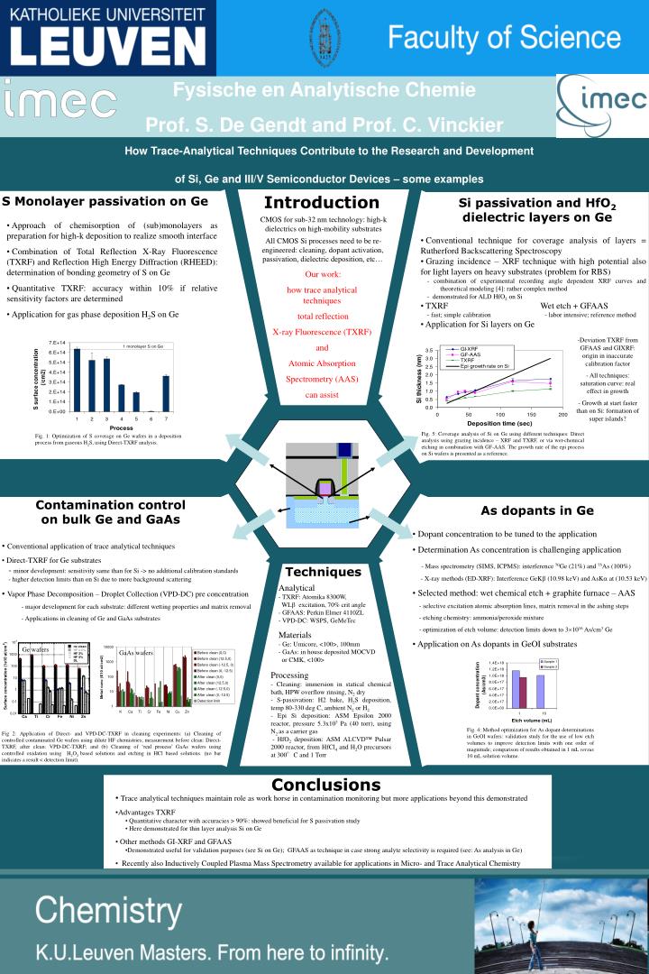
Fig. 5: Coverage analysis of Si on Ge using different techniques: Direct analysis using grazing incidence – XRF and TXRF, or via wet-chemical etching in combination with GF-AAS. The growth rate of the epi process on Si wafers is presented as a reference.

E N D
Fig. 5: Coverage analysis of Si on Ge using different techniques: Direct analysis using grazing incidence – XRF and TXRF, or via wet-chemical etching in combination with GF-AAS. The growth rate of the epi process on Si wafers is presented as a reference. Fig. 1: Optimization of S coverage on Ge wafers in a deposition process from gaseous H2S, using Direct-TXRF analysis. Fig. 4: Method optimization for As dopant determinations in GeOI wafers: validation study for the use of low etch volumes to improve detection limits with one order of magnitude; comparison of results obtained in 1 mL versus 10 mL solution volume. Fysische en Analytische Chemie Prof. S. De Gendt and Prof. C. Vinckier How Trace-Analytical Techniques Contribute to the Research and Development of Si, Ge and III/V Semiconductor Devices – some examples Introduction S Monolayer passivation on Ge Si passivation and HfO2 dielectric layers on Ge CMOS for sub-32 nm technology: high-k dielectrics on high-mobility substrates • Approach of chemisorption of (sub)monolayers as preparation for high-k deposition to realize smooth interface • Combination of Total Reflection X-Ray Fluorescence (TXRF) and Reflection High Energy Diffraction (RHEED): determination of bonding geometry of S on Ge • Quantitative TXRF: accuracy within 10% if relative sensitivity factors are determined • Application for gas phase deposition H2S on Ge • Conventional technique for coverage analysis of layers = Rutherford Backscattering Spectroscopy • Grazing incidence – XRF technique with high potential also for light layers on heavy substrates (problem for RBS) • - combination of experimental recording angle dependent XRF curves and theoretical modeling [4]: rather complex method • - demonstrated for ALD HfO2 on Si • TXRF Wet etch + GFAAS • - fast; simple calibration - labor intensive; reference method • Application for Si layers on Ge All CMOS Si processes need to be re-engineered: cleaning, dopant activation, passivation, dielectric deposition, etc… Our work: how trace analytical techniques total reflection X-ray Fluorescence (TXRF) and Atomic Absorption Spectrometry (AAS) can assist • Deviation TXRF from GFAAS and GIXRF: origin in inaccurate calibration factor • All techniques: saturation curve: real effect in growth • Growth at start faster than on Si: formation of super islands? Contamination control on bulk Ge and GaAs As dopants in Ge • Dopant concentration to be tuned to the application • Determination As concentration is challenging application • - Mass spectrometry (SIMS, ICPMS): interference 70Ge (21%) and 75As (100%) • - X-ray methods (ED-XRF): Interference GeK (10.98 keV) and AsK at (10.53 keV) • Selected method: wet chemical etch + graphite furnace – AAS • - selective excitation atomic absorption lines, matrix removal in the ashing steps • - etching chemistry: ammonia/peroxide mixture • - optimization of etch volume: detection limits down to 31016 As/cm3 Ge • Application on As dopants in GeOI substrates • Conventional application of trace analytical techniques • Direct-TXRF for Ge substrates • - minor development: sensitivity same than for Si -> no additional calibration standards • - higher detection limits than on Si due to more background scattering • Vapor Phase Decomposition – Droplet Collection (VPD-DC) pre concentration • - major development for each substrate: different wetting properties and matrix removal • Applications in cleaning of Ge and GaAs substrates Techniques • Analytical • TXRF: Atomika 8300W, • WL excitation, 70% crit angle • - GFAAS: Perkin Elmer 4110ZL • - VPD-DC: WSPS, GeMeTec • Materials • - Ge: Umicore, <100>, 100mm • GaAs: in house deposited MOCVD • or CMK, <100> Ge wafers GaAs wafers Processing - Cleaning: immersion in statical chemical bath, HPW overflow rinsing, N2 dry - S-passivation: H2 bake, H2S deposition, temp 80-330 deg C, ambient N2 or H2 - Epi Si deposition: ASM Epsilon 2000 reactor, pressure 5.3x10³ Pa (40 torr), using N2 as a carrier gas - HfO2 deposition: ASM ALCVD™ Pulsar 2000 reactor, from HfCl4 and H2O precursors at 300°C and 1 Torr Fig 2: Application of Direct- and VPD-DC-TXRF in cleaning experiments: (a) Cleaning of controlled contaminated Ge wafers using dilute HF chemistries; measurement before clean: Direct-TXRF, after clean: VPD-DC-TXRF; and (b) Cleaning of ‘real process’ GaAs wafers using controlled oxidation using H2O2 based solutions and etching in HCl based solutions. (no bar indicates a result < detection limit). Conclusions • Trace analytical techniques maintain role as work horse in contamination monitoring but more applications beyond this demonstrated • Advantages TXRF • Quantitative character with accuracies > 90%: showed beneficial for S passivation study • Here demonstrated for thin layer analysis Si on Ge • Other methods GI-XRF and GFAAS • Demonstrated useful for validation purposes (see Si on Ge); GFAAS as technique in case strong analyte selectivity is required (see: As analysis in Ge) • Recently also Inductively Coupled Plasma Mass Spectrometry available for applications in Micro- and Trace Analytical Chemistry