Download
1 / 29
290 likes | 482 Vues
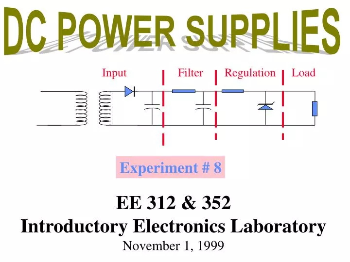
Input. Filter. Regulation. Load. Experiment # 8. EE 312 & 352 Introductory Electronics Laboratory November 1, 1999. Objective:.

E N D
Input Filter Regulation Load Experiment # 8 EE 312 & 352 Introductory Electronics Laboratory November 1, 1999
Objective: • Design, construct, and test a dc power supply. The power supply includes a transformer, diodes, and a filter. All were investigated in previous experiments. This the major design project in the course.
Input: 120 VAC RMS, 60 Hz Steps the input voltage up and down as needed Convert the ac to a pulsing dc Low-pass type for removing voltage variation Keeps voltage constant regardless of load change DC-VOLTAGE POWER SUPPLY OPERATION Alternator or Power Company Load Transformer Rectifier Filter Regulator v t
Power Company v 167 118 Vrms 16.7 ms or 60Hz t Load Transformer Rectifier Filter Regulator
Alternator or Power Company v 25.5 18 Vrms 16.7 ms or 60Hz t Load Transformer Rectifier Filter Regulator v 118 Vrms 167 16.7 ms or 60Hz t
Alternator or Power Company v RLoad t half-wave rectifier Load Transformer Rectifier Filter Regulator 60Hz RLoad 120Hz v t RLoad full-wave rectifier
Alternator or Power Company v 18 Vrms 25.5 16.7 ms or 60Hz t Load Transformer Rectifier Filter Regulator v 60 Hz ~ 0.6V 24.9 12.45 Vrms t t half-wave rectifier
Alternator or Power Company Load Transformer Rectifier Filter Regulator Input Filter Regulation Load stage 1 stage 2
v v ripple Vmax t t t t Input Filter Regulation Load C stage 1 without C with C
? v Vmax ? ripple VDC 0 t t
Input Filter Regulation Load R C Vinput V across R < 25% of Vinput stage 2 One or more filter sections are usually used to reduce the amplitude of the ripple. The filter used in this experiment is a single-section low-pass RC filter. usually tolerable
Ripple Reduction Factor: Vout Vin
Alternator or Power Company Load Transformer Rectifier Filter Regulator You are asked to design and built a 12 V dc regulated power supply. In this experiment you use a Zener diode that breaks down at 12 V.
Forward Characteristics 12Volts breakdown voltage ID VD Reverse Characteristics ~ ~ IMax IDC ILoad Iz Iz
Rs IDC ILoad RLoad Rz Iz ID VD ~ ~ IMax Voltage Divider IDC Rs ILoad = Vinput Rz RLoad Iz
Summary Alternator or Power Company Load Transformer Rectifier Filter Regulator v t
Procedures: I- Design, construct, and test a dc power supply. II- Simulate dc power supply. I
Components: • 18 Volts Transformer • Variac • Bridge rectifier (use 1 diode) • Zener diode (Vbd=12Vdc, 1N4742) • 12 Watt, 1000 Ohm, variable resistor • 2 Resistor Substitution Boxes • 50, 100, and 200 UF Fixed Capacitors
R? R? ILoad = 50mA VLoad =12 V dc R? C? C? Peak to peak ripple voltage from the input stage < 20% Peak to peak ripple voltage at the load <= 1% 1- Design, construct, test a dc power supply Suggestion: Zener diode current = 21 mA (At this current, the Zener resistance is 9 ohms)
ILoad = 50mA R? R? VLoad =12 V dc RLoad? C? C? Peak to peak ripple voltage from the input stage < 20% Peak to peak ripple voltage at the load <= 1%
IDC ILoad = 50mA IDC R? R? VLoad =12 V dc C? C? Iz=21mA Peak to peak ripple voltage from the input stage < 20% Peak to peak ripple voltage at the load <= 1%
IDC=71mA ILoad = 50mA R? R? VLoad =12 V dc CI? C? Iz=21mA Peak to peak ripple voltage from the input stage < 20% Peak to peak ripple voltage at the load <= 1% v Vmax ripple VDC 0 t t
20% ripple Vmax = 24.9 v < 24.9 x 0.2=4.98 V ripple VDC=22.4 V Vmin=19.92 0 t t
IDC=71mA ILoad = 50mA RF? Rs? VLoad =12 V dc CF? CI=250uF Iz=21mA Peak to peak ripple voltage at the load <= 1% VDC=0.6V+IDC(RF+RS)+Vz 22.4=0.6+.071(RF+RS)+12 RF+RS = 138.03 ohms
IDC=71mA ILoad = 50mA RF? Rs? VLoad =12 V dc CF? CI=250uF Iz=21mA Peak to peak ripple voltage at the load <= 1% 6.6% ripple 20% ripple &
IDC=71mA ILoad = 50mA RF=75 Rs=63 VLoad =12 V dc CI=250uF CF=250uF Iz=21mA Peak to peak ripple voltage at the load <= 1% 2% ripple 0.1% ripple
2- Simulation of Part I Simulate the dc power supply! Show output wave form at points 1, 2, and 3. Comnpare these waveforms with your experiment. 1 2 3
? RF=105 Rs=33 ILoad = 50mA VLoad =12 V dc CI=250uF CF=250uF Iz=21mA Transformer 18.0 V 118.4 V variable Variac
Report is required for EE 312 & 352