Download
1 / 37
380 likes | 658 Vues
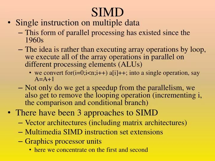
SIMD. Single instruction on multiple data This form of parallel processing has existed since the 1960s T he idea is rather than executing array operations by loop, we execute all of the array operations in parallel on different processing elements (ALUs)

E N D
SIMD • Single instruction on multiple data • This form of parallel processing has existed since the 1960s • The idea is rather than executing array operations by loop, we execute all of the array operations in parallel on different processing elements (ALUs) • we convert for(i=0;i<n;i++) a[i]++; into a single operation, say A=A+1 • Not only do we get a speedup from the parallelism, we also get to remove the looping operation (incrementing i, the comparison and conditional branch) • There have been 3 approaches to SIMD • Vector architectures (including matrix architectures) • Multimedia SIMD instruction set extensions • Graphics processor units • here we concentrate on the first and second
Two Views • If we have n processing elements • we view the CPU as having a control unit and n ALUs (processing elements, or PEs in the figure) • each PE handles 1 datum from the array where data is cached in a PE’s local cache • Otherwise, we use pipelined functional units • rather than executing the instruction on n data simultaneously, in each cycle we start the next array operation in the functional unit pipeline
The Pipelined Approach • Although the simultaneous execution provides the more efficient execution, the pipelined approach is preferred in modern architectures for several reasons • It is a lot cheaper than having n PEs • We already have pipelined functional units so the vector processing does not require a significant change to our ALU • The simultaneous execution is limited to n parallel operations per cycle because of the limitation in PEs and so we still may need to execute the looping mechanism • e.g., a loop of 100 array elements on an architecture of 8 PEs still needs the loop to iterate 13 times • There is no need to support numerous individual caches with parallel access • although we will use multi-banked caches • Requires less power utilization which is significant today
VMIPS • We alter MIPS to now support vector operations • The idea is that we will combine array elements into storage so that we can fetch several array elements in one cycle from memory (cache) and store them in large (wide) registers • we will use vector registers where one register stores multiple array elements, a portion of the entire array • This requires widening the bus and also costs us in terms of greater memory access times because we are retrieving numerous words at a time • in VMIPS, a register can store 64 elements of 64-bit items and there are 8 such registers • additionally, there are scalar registers (32 integer and 32 FP) • the registers all connect via ports to all of the functional units as well as the load/store unit, there are numerous ports to support parallel data movement (see slide 2 or figure 4.2 page 265)
VMIPS Instruction Set • Aside from the ordinary MIPS instructions (scalar operations), we enhance MIPS with the following: • LV, SV – load vector, store vector • LV V1, R1 – load vector register V1 with the data starting at the memory location stored in R1 • also LVI/SVI for using indexed addressing mode, and LVWS and SVWS for using scaled addressing mode • ADDVV.D V1, V2, V3 (V1 V2 + V3) • ADDVS.D V1, V2, F0 (scalar addition) • similarly for SUB, MUL and DIV • S--VV.D V1, V2 and S--VS.D V1, F0 to compare pairwise elements in V1 and V2 or V1 and F0 • -- is one of EQ, NE, GT, LT, GE, LE • result of comparison is a set of boolean values placed into the bit vector register VM which we can then use to implement if statements • POP R1, VM – count number of 1s in the VM and store in R1 • this is only a partial list of instructions, and only the FP operations, see figure 4.3 for more detail, missing are any integer based operations
Example • Let’s look at a typical vector processing problem, computing Y = a*X + Y • Where X & Y are vectors and a is a scalar (e.g., y[i]=y[i]+a*x[i]) • The MIPS code is on the left and the VMIPS code is on the right L.D F0, a DADDI R4, Rx, #512 Loop: L.D F2, 0(Rx) MUL.D F2, F2, F0 L.D F4, 0(Ry) ADD.D F4, F4, F2 S.D F4, 0(Ry) DADDI Rx, Rx, #8 DADDI Ry, Ry, #8 DSUB R20, R4, Rx BNEZ R20, Loop L.D F0, a LV V1, Rx MULVS.D V2, V1, F0 LV V3, Ry ADDVV.D V4, V2, V3 SV V4, Ry In MIPS, we execute almost 600 instructions whereas in VMIPS, only 6 (there are 64 elements in the array to process, each is 8 bytes long) and there are no RAW hazards or control hazards to deal with
Vector Execution Time • Although we typically compute execution time in seconds (ns) or clock cycles, for vector operations, architects are more interested in the number of distinct issues required to execute some chunk of code • This requires some explanation • The vector processor’s performance is impacted by the length of the vector (the number of array values stored in a single vector), any structural hazards (caused by limitations to the number and type of functional units) and data dependencies between vectors • we will ignore the last one, at least for now • The vector processor’s performance then is primarily based on the length of the vector • for instance, in VMIPS, our vector length is 64 doubles, but if our vector stores 128 doubles, then we have to do our vector operation twice
Convoys and Chimes • A convoy is a set of sequential vector operations that can be issued together without a structural hazard • Because we are operating on vectors in a pipeline, the execution of these operations can be overlapped • e.g., L.V V1, Rx followed by ADDVV.D V3, V1, V2 would allow us to retrieve the first element of V1 and then start the addition while retrieving the second element of V1 • A chime is the amount of time it takes to execute a convoy • We will assume that there are no stalls in executing the convoy, so the chime will take n + x – 1 cycles where x is the length of the convoy and n is the number of data in the vector • A program of m convoys will take m chimes, or m * (n + x – 1) cycles (again, assuming no stalls) • The chime time ignores pipeline overhead, and so architects prefer to discuss performance in chimes
Convoy Example • Assume we have 1 functional unit for each operation (load/store, add, multiply, divide) • We have the following VMIPS code executing on a vector of 64 doubles • LV V1, Rx • MULVS.D V2, V1, F0 • LV V3, Ry • ADDVV.D V4, V2, V3 • SV V4, Ry • The first LV and MULVS.D can be paired in a convoy, but not the next LV because there is only 1 load unit • Similarly, the second LV and ADDVV.D are paired but not the final SV • This gives us 3 convoys: • LV MULVS.D • LV ADDVV.D • SV
Multiple Lanes • The original idea behind SIMD was to have n PEs so that n vector elements could be executed at the same time • We can combine the pipeline and the n PEs, in which case, the parallel functional units are referred to as lanes • Without lanes, we launch 1 FP operation per cycle in our pipelined functional unit • With lanes, we launch n FP operations per cycle, one per lane, where elements are placed in a lane based on their index • for instance, if we have 4 lanes, lane 0 gets all elements with index i % 4 == 0 whereas lane 1 gets all elements with i % 4 == 1 • To support lanes, we need lengthy vectors • If our vector is 64 doubles and we have 16 lanes on a 7 cycle multiply functional unit, then we are issuing 16 instructions per cycle over 4 cycles and before we finish the first multiplies, we are out of data, so we don’t get full advantage of the pipelined nature of the functional units! • We also need multi-banked caches to permit multiple loads/stores per cycle to keep up with the lanes
Handling Vectors > 64 Elements • The obvious question with respect to SIMD is what happens if our vector’s length > the size of our vector register (which we will call maximum vector length or MVL) • If this is the case, then we have to issue the vector code multiple times, in a loop • by resorting to using a loop, we lose some of the advantage – no branch penalties or loop mechanisms • On the other hand, we cannot provide an infinitely long (or ridiculously long) vector register in hopes to satisfy all array usage • Strip mining is the process of generating code to handle such a loop in which the number of loop iterations is n / MVL where n is the size of the program’s vector • Note: if n / MVL leaves a remainder then our last iteration will take place on only a partial vector • see the discussion on pages 274-275 for more detail
Handling If Statements LV V1, Rx LV V2, Ry L.D F0, #0 SNEVS.D V1, F0 SUBVV.D V1, V2, V2 SV V1, Rx • As with loop unrolling, if our vector code employs if statements, we can find this a challenge to deal with • Consider for instance • for(i=0;i<n;i++) • if(x[i] != 0) • x[i]=x[i] – y[i]; • We cannot launch the subtraction down the FP adder functional unit until we know the result of the condition • In order to handle such a problem, vector processors use a vector mask register • The condition is applied in a pipelined unit creating a list of 1s and 0s, one per vector element • This is stored in the VM (vector mask) register • Vector mask operations are available so that the functional unit only executes on vector elements where the corresponding mask bit is 1 Notice SUBVV.D is a normal subtract instruction -- we need to modify it to execute using the vector mask
Memory Bank Support • We will use non-blocking caches with critical word first/early restart • However, that does not necessarily guarantee 1 vector element per cycle to keep up with the pipelined functional unit because we may not have enough banks to accommodate the MVL • the Cray T90 has 32 processors, each capable of generating up to 4 loads and 2 stores per clock cycle • the processor’s clock cycle is 2.167 ns and cache has a response time of 15 ns • to support the full performance of the processor, we need 15 / 2.167 * 32 * (4 + 2) = 1344 individual accesses per cycle, thus 1344 banks! It actually has 1024 banks (altering the SRAM to permit pipelined accesses makes up for this)
Strides • Notice that the vector registers store consecutive memory locations (e.g., a[i], a[i+1], a[i+2], …) • In some cases, code does not visit array locations in sequential order, this is especially problematic in 2-D array code • a[i][j]=a[i][j] + b[i][k] * d[k][j] • A stride is the distance separating elements in a given operation • The optimal stride is 1 but for the above code, we would either have difficulty when accessing b[i][k] or d[k][j] depending on loop ordering resulting in a stride of as large as 100 • The larger the stride, the less effective the vector operations may be because multiple vector register loads will be needed cycle-after-cycle • blocking (refer back to one of the compiler optimizations for cache) can be used to reduce the impact • To support reducing such an impact, we use cache banks and also a vector load that loads vector elements based on strides rather than consecutive elements
SIMD Extensions for Multimedia • When processors began to include graphics instructions, architects realized that operations not necessarily need to be 32-bit instructions • Graphics for instance often operates on several 8-bit operations (one each for red, green, blue, transparency) • so while a datum might be 32 bits in length, it really codified 4 pieces of data, each of which could be operated on simultaneously within the adder • Additionally, sounds are typically stored as segments of 8 or 16 bit data • Thus, vector SIMD operations were incorporated into early MMX style architectures • This did not require additional hardware, just new instructions to take advantage of the hardware already available
Instructions • Unsigned add/subt • Maximum/minimum • Average • Shift right/left • These all allow for 32 8-bit, 16 16-bit, 8 32-bit or 4 64-bit operations • Floating point • 16 16-bit, 8 32-bit, 4 64-bit or 2 128-bit • Usually no conditional execution instructions because there would not necessarily be a vector mask register • No sophisticated addressing modes to permit strides (or deal with sparse matrices, a topic we skipped) • The MMX extension to x86 architectures introduced hundreds of new instructions • The streaming SIMD extensions (SSE) to x86 in 1999 added 128-bit wide registers and the advanced vector extensions (AVD) in 2010 added 256-bit registers
Example L.D F0, a MOV F1, F0 MOV F2, F0 MOV F3, F0 DADDI R4, Rx, #512 Loop: L.4D F4, 0(Rx) MUL.4D F4, F4, F0 L.4D F8, 0(Ry) ADD.4D F8, F8, F4 S.4D F8, 0(Rx) DADDI Rx, Rx, #32 DADDI Ry, Ry, #32 DSUB R20, R4, Rx BNEZ R20, Loop • In this example, we use a 256-bit SIMD MIPS • The 4D suffix implies 4 doubles per instruction • The 4 doubles are operated on in parallel • either because the FP unit is wide enough to accommodate 256 bits or because there are 4 parallel FP units The 4D extension used with register F0 Means that we are actually using F0, F1, F2, F3 combined L.4D/S.4D moves 4 array elements at a time
TLP: Multiprocessor Architectures • In chapter 3, we looked at ways to directly support threads in a processor, here we expand our view to multiple processors • We will differentiate among them as follows • Multiple cores • Multiple processors each with one core • Multiple processors each with multiple cores • And whether the processors/cores share memory • When processors share memory, they are known as tightly coupled and they can promote two types of parallelism • Parallel processing of multiple threads (or processes) which are collaborating on a single task • Request-level parallelism which has relatively independent processes running on separate processors (sometimes called multiprogramming)
Shared Memory Architecture • We commonly refer to this type of architecture as symmetric multiprocessors (SMP) • Tightly coupled, or shared memory • also known as a uniform memory access multiprocessor • Probably only a few processors in this architecture (no more than 8 or shared memory becomes a bottleneck) Although in the past, multiprocessor computers could fall into this category, today we typically view this category as a multicore processor, true multiprocessor computers will use distributed memory instead of shared memory
Challenges • How much parallelism exists within a single program to take advantage of the multiple processors? • Within this challenge, we want to minimize the communication that will arise between processors (or cores) because the latency is so much higher than the latency of a typical memory access • we wish to achieve an 80 times speedup from 100 processors , using Amdahl’s Law, compute the amount of time the processors must be working on their own (not communicating together). Solution: 99.75% of the time (solution on page 349) • What is the impact of the latency of communication? • we have 32 processors and a 200 ns time for communication latency which stalls the processor, if the processor’s clock rate is 3.3 GHz and the ideal CPI is .5, how much faster is a machine with no interprocess communication versus one that spends .2% of the time communicating? 3.4 times faster (solution on page 350)
Cache Coherence • The most challenging aspect of a shared memory architecture is ensuring data coherence across processors • What happens if two processors both read the same datum? If one changes the datum, the other has a stale value, how do we alert it to update the value? • As an example, consider the following time line of events
Cache Coherence Problem • We need our memory system to be both coherent and consistent • A memory system is coherent if • a read by processor P to X followed by a write of P to X with no writes of X by any other processor always returns the value written by P • a read by a processor to X following a write by another processor to X returns the written value if the read and write are separated by a sufficient amount of time • writes to the same location are serialized so that the writes are seen by all processors in the same order • Consistency determines when a written value will be returned by a later read • we will assume that a write is only complete once that write becomes available to all processors (that is, a write to a local cache does not mean a write has completed, the write must also be made to shared memory) • if two writes take place, to X and Y, then all processors must see the two writes in the same order (X first and then Y for instance)
Snooping Coherence Protocol • In an SMP, all of the processors have caches which are connected to a common bus • The snoopy cache listens to the bus for write updates • Data falls into one of these categories • Shared – datum that can be read by anyone and is valid • Modified – datum has been modified by this processor and must be updated on all other processors • Invalid – data has been modified by another processor but not yet updated by this cache • The snooping protocol has two alternatives • Write-invalidate – upon a write, the other caches must mark their own copies as invalid and retrieve the updated datum before using it • it two processors attempt to write at the same time, only one wins, the other must invalidate its write, obtain the new datum and then reperform its operation(s) on the new datum • Write-update – upon a write, update all other caches at the same time by broadcasting the new datum
Extensions to Protocol • MESI – adds a state called Exclusive • If a datum is exclusive to the cache, it can be written without generating an invalidate message to the bus • If a read miss occurs to a datum that is exclusive to a cache, then the cache must intercept the miss, send the datum to the requesting cache and modify the state to S (shared) • MOESI – adds a state called Owned • In this case, the cache owns the datum AND the datum is out of date in memory (hasn’t been written back yet) • This cache MUST respond to any requests for the datum since memory is out of date • But the advantage is that if a modified block is known to be exclusive, it can be changed to Owned to avoid writing back to memory at this time
A Variation of the SMP • As before, each processor has its own L1 and L2 caches • snooping must occur at the interconnection network in order to modify the L1/L2 caches • A shared L3 cache is banked to improve performance • The shared memory level is the backup to L3 as usual and is also banked
Performance for Shared Memory • Here, we concentrate just on memory accesses of a multicore processor with a snoopy protocol (not the performance of the processors themselves) • Overall cache performance is a combination of • miss rate as derived from compulsory, conflict and capacity misses (these misses are sometimes called true sharing misses) • traffic from communication including invalidations and cache misses after invalidations, these are sometimes referred to as coherence misses (these misses are sometimes called false sharing misses) • Example • Assume that x1 and x2 are in the same cache block and are shared by P1 and P2, indicate the true and false misses and hits from below: • P1 P2 • write x1 – true (P1 must send out invalidate signal) • read x2 – false (block was invalidated) • write x1 – false (block marked as shared because of P2’s read of x2) • write x2 – false (block marked as shared with P1) • read x2 – true (need new value from P2)
Commercial Workloads • To demonstrate the performance of the snoopy cache protocol on a SMP, we look at a study done on the DEC ALPHA 21164 from 1998 • 4 processors (from 1998) with each processor issuing up to 4 instr/clock cycle, 3 levels of cache • L1: 8 KB/8 KB instr/data cache, direct-mapped, 32 byte blocks, 7 cycle miss penalty • L2: 96 KB, 3 way set assoc, 32 byte block, 21 cycles • L3: 2 MB, direct mapped, 64 byte block, 80 cycle miss • As a point of comparison, the Intel i7 has these three caches • L1: 32 KB/32 KB instr/data cache, 4 way/8 way, 64 byte blocks, 10 cycle miss penalty • L2: 256 KB, 8 way set assoc, 64 byte block, 35 cycles • L3: 2 MB (per core), 16 way, 64 byte block, 100 cycle miss • The study looks at 3 benchmarks: • OLTP - user mode 71%, kernel time 18%, idle 11% • DSS – 87%, 4%, 9% • AltaVista (search engine) – 98%, <1%, <1%
Distributed Shared Memory • The tightly coupled (shared memory) multiprocessor is useful for promoting parallelism within tasks (whether 1 process, a group of threads, or related processes) • However, when processes generally will not communicate with each other, there is little need to force the architect to build a shared memory system • The loosely coupled, or distributed memory system, is generally easier to construct and possibly cheaper • in fact, any network of computers can be thought of as a loosely coupled multiprocessor • Any multicore multiprocessor will be of this configuration
DSM Architecture • Here, each multicore MP is a SMP as per our previous slides • Connecting each processor together is an interconnection network • An example ICN is shown to the right, there are many topologies including nearest neighbors of 1-D, 2-D, 3-D and hypercubes
Directory-based Protocol • The snoopy protocol requires that caches broadcast invalidates to other caches • For a DSM, this is not practical because of the lengthy latencies in communication • Further, there is no central bus that all processors are listening to for such messages (the ICN is at a lower level of the hierarchy, passed the caches but possibly before a shared memory) • So the DSM requires a different form for handling coherence, so we turn to the directory-based protocol • We keep track of every block that may be cached in a central repository called a directory • This directory maintains information for each block: • in which caches it is stored • whether it is dirty • who currently “owns” the block
The Basics of the Protocol • Cache blocks will have one of three states • Shared – one or more nodes currently have the block that contains the datum and the value is up to date in all caches and main memory • Uncached – no node currently has the datum, only memory • Modified – the datum has been modified by one node, called the owner • for a node to modify a datum, it must be the only node to store the datum, so this permits exclusivity • if a node intends to modify a shared datum, it must first seek to own the datum from the other caches, this allows a node to modify a datum without concern that the datum is being or has been modified by another node in the time it takes to share the communication • once modified, the datum in memory (and any other cache) is invalid, or dirty
The Directory(ies) • The idea is to have a single directory which is responsible for keeping track of every block • But it is impractical to use a single directory because such an approach is not scalable • Therefore, the directory must be distributed • Refer back to the figure 3 slides ago, we enhance this by adding a directory to each MP • each MP now has its multicores & L1/L2 caches, a shared L3 cache, I/O, and a directory • The local directory consists of 1 entry per block in the caches (assuming we are dealing with multicore processors and not collections of processors) • we differentiate between the local node (the one making a request) and the home node (the node storing or owning the datum) and a remote node (a node that has requested an item from the owner or a node that requires invalidation once the owner has modified the datum)