Download
1 / 11
110 likes | 248 Vues
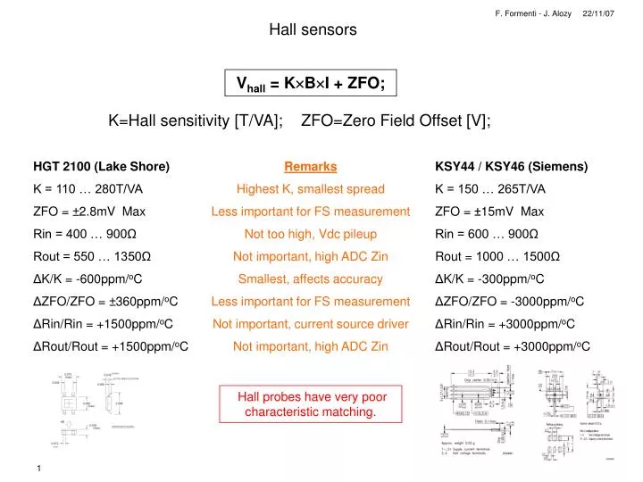
Hall sensors. V hall = K B I + ZFO;. K=Hall sensitivity [T/VA]; ZFO=Zero Field Offset [V];. HGT 2100 (Lake Shore) K = 110 … 280T/VA ZFO = ±2.8mV Max Rin = 400 … 900 Ω Rout = 550 … 1350 Ω Δ K/K = -600ppm/ o C Δ ZFO/ZFO = ±360ppm/ o C Δ Rin/Rin = +1500ppm/ o C

E N D
Hall sensors Vhall = KBI + ZFO; K=Hall sensitivity [T/VA]; ZFO=Zero Field Offset [V]; HGT 2100 (Lake Shore) K = 110 … 280T/VA ZFO = ±2.8mV Max Rin = 400 … 900Ω Rout = 550 … 1350Ω ΔK/K = -600ppm/oC ΔZFO/ZFO = ±360ppm/oC ΔRin/Rin = +1500ppm/oC ΔRout/Rout = +1500ppm/oC Remarks Highest K, smallest spread Less important for FS measurement Not too high, Vdc pileup Not important, high ADC Zin Smallest, affects accuracy Less important for FS measurement Not important, current source driver Not important, high ADC Zin KSY44 / KSY46 (Siemens) K = 150 … 265T/VA ZFO = ±15mV Max Rin = 600 … 900Ω Rout = 1000 … 1500Ω ΔK/K = -300ppm/oC ΔZFO/ZFO = -3000ppm/oC ΔRin/Rin = +3000ppm/oC ΔRout/Rout = +3000ppm/oC Hall probes have very poor characteristic matching.
Vcm=Vdc Vcm=2Vdc Vcm=3Vdc I Rin Rin Rin Vdc Vdc Vdc Hall sensors • Best I bias is when getting closer to ADC full scale, at measured B: • Ex. HGT 2100, B=1T, FS=100mV => I = 0.36mA … 0.9mA • Ex. HGT 2100, B=1T, FS=1V => I = 3.6mA … 9mA • Using common I bias => I bias is set for worst case, i.e. highest K, loosing accuracy for lowest K • Do select Hall probes? Possible from manufacturer? Cost? • Using independent I biases => I bias can always be set for optimal case, i.e. FS range • Easy to equalize probes (i.e. large dispersion of K parameter) through I bias adjust • Additional constraint for probes in series is Vdc pileup vs. Rin and I bias: • Ex. 3 x HGT 2100, Rin=400…900Ω, I = 0.36mA … 0.9mA => Vpileup=0.43V…2.4V • BUT: ADC Max IN Common Mode Voltage = 0.95V on FS=100mV • I bias shall not be too low, to make sure that effect of ZFO is negligible vs. KBI: • Ex. HGT 2100, B=1T, FS=100mV => fix ZFO < KBI /10 => I > 0.1mA … 0.25mA • Compatible with above cases of FS=100mV and FS=1V • I bias shall not be too high, to limit temperature effect => case of FS=1V and I=9mA may be excessive FS 100mV looks a good compromise for the case of B=1T
Ibias R Load - Vref = 2.5V + 5µV Max + Vofs - Current source • Use of ZeroDrift series AmpOp => OPA335 • Auto-zeroing technique to provide very low offset and zero drift over time and temperature • Vofs = 5µV Max • ΔVofs/Vofs = 100ppm Max • Vout margin from supply rails = 100mV Max • Very good dispersion characteristic vs. production • Very low impact of Vofs over Ibias Ibias = (Vref-Vofs)/R ΔIbias/Ibias = Vofs/Vref = 2ppm Max • Ibias matching assured by resistor value tolerance=>0.1% (0.01% also possible on request) • This is much better than Hall probe sensitivity matching (ΔK = 155%) • Resistor thermal stability = Vref thermal stability = 5ppm/oC=> to compare with ΔK/K = 600ppm/oC No problems to use three independent current sources
50µV 50µV (Channel with inverted polarity) Current source • B-Field card with three different Ibias and Rload = 249Ω(NOTE: it also includes temp variation of Rload) Slope differences correspond to different resistor temperature coefficients: optimal resistor temperature coefficient can be adopted. • B-Field card with three equal Ibias and Rload = 249Ω(NOTE: it also includes temp variation of Rload) Three ADC channels behave in equal manner with equal resistors: good characteristic matching among channels.
ADC Low Ranges (25mV … 100mV) • Analog Input Common Mode: 1.85V 2.65V 0.8V NBV at GND => 0V High Ranges (1V … 5V) 5V Vcm=2.5V Low Ranges (25mV … 100mV) - 0.15V 0.95V 1.1V NBV = -1.8V … -2.5V => 0V High Ranges (1V … 5V) 5V • For best noise performance, it is better to Ground NBV (no charge pump) => Set IN Common Mode = 2.5V to assure compatibility for Low and High Ranges. => V Hall probes pileup = 0.43V … 2.4V 0.8V not enough to safely accommodate 3 probes in series and have FS measurement. • System channel calibration => It is more effective than self calibration System Calibration Self Calibration System calibration will be implemented
ADC Increasing FS range=> moderately improves S/N Slowing output rate (longer conversion time) => improves S/N 100mV and 1V FS ranges behave in similar way w.r.t S/N
Mean = -252.421mV; σ = 4.93µV Mean = -123.374mV; σ = 4.34µV Mean = -632.574mV; σ = 5.00µV Noise free resolution (16 bits) 28 LSB counts 6σ = 30µV σ5µV 10 LSB 1.2µV ADC • DC Vin acquisition statistics (1000 samples) at 1V range, without hall probes and three different I bias Measured ADC S/N performance – for minimal relative error, measurement has to be done closest to FS • Example of 1000 samples acquisition LSB = 2V / 224 0.12µV (bipolar mode, 1V range) Accuracy 310-5 of FS (single acquisition, 15Hz) Recording the average, the accuracy improves of √1000 30 times (30µV -> 1µV, i.e. 10-6)
ADC • Offset measurement at constant Temperature Average fit = best calibration value Channel calibration (offset and gain) must be done by averaging samples, not on single acquisition
Voltage reference • LT1019A Linear Technology. • B-field circuit architecture is conceived to be only dependent on Vref accuracy and stability. • 2.5V nominal voltage • 0.05% Max accuracy (i.e. 1.25mV Max) • (compensation of relative variations of ADC LSB amplitude and Hall probe voltage gain) • 5ppm/oC Max, over 0oC … 70oC (i.e. 0.875mV Max over 70oC) (same as precision resistors) • Tests with a 5ppm/oC to 20ppm/oC reference and external Vin source. 9µV/oC i.e. 10ppm/oC A stable voltage reference is important for the performance
Temperature sensor • Test with two temperature sensors: inside the Voltage reference (LT1019) and on board (DS60) LT1019 => Temp coeff 2.1mV/oC NOTE: absolute temperature depends from process => applicable only for relative temperature change measurement DS60 => Temp coeff 6.25mV/oC (6.0mV/oC … 6.5mV/oC) and 424mV offset at 0oC Accuracy = ±2oC (guaranteed stable on long term) Both sensors have good linearity 6.44mV/oC 2.15mV/oC A precise temperature sensor for absolute temperature measurement is necessary
Conclusions • Sensor card (electronics) works according datasheet expectations. • For best performance select very good Vref, some stable resistors and a precise temp sensor. • Accuracy of 10-4 Max (electronics) can be guaranteed through single data acquisition (FS measurement). • ADC system calibration gives better results than self calibration. • Hall probes need equalization for best channel accuracy. • Performance vs. temperature has not yet been checked w.r.t. datasheet • Sensor card (electronics) temperature test resulted in 10ppm/oC drift (range 20oC to 65oC). • Better (<10-4) accuracy (electronics) can be achieved either: • by lowering ADC output rate (higher S/N, slower readout) • through over-sampling and averaging technique (can extend limitation of min out rate)