Download
1 / 20
210 likes | 225 Vues
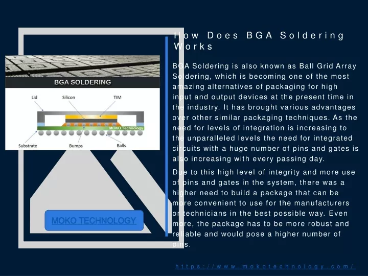
BGA Soldering is also known as Ball Grid Array Soldering, which is becoming one of the most amazing alternatives of packaging for high input and output devices at the present time in the industry. It has brought various advantages over other similar packaging techniques. As the need for levels of integration is increasing to the unparalleled levels the need for integrated circuits with a huge number of pins and gates is also increasing with every passing day.<br>Due to this high level of integrity and more use of pins and gates in the system, there was a higher need to build a package that can be more convenient to use for the manufacturers or technicians in the best possible way. Even more, the package has to be more robust and reliable and would pose a higher number of pins.<br><br>

E N D
How Does BGA Soldering Works BGA Soldering is also known as Ball Grid Array Soldering, which is becoming one of the most amazing alternatives of packaging for high input and output devices at the present time in the industry. It has brought various advantages over other similar packaging techniques. As the need for levels of integration is increasing to the unparalleled levels the need for integrated circuits with a huge number of pins and gates is also increasing with every passing day. Due to this high level of integrity and more use of pins and gates in the system, there was a higher need to build a package that can be more convenient to use for the manufacturers or technicians in the best possible way. Even more, the package has to be more robust and reliable and would pose a higher number of pins. MOKO TECHNOLOGY https://www.mokotechnology.com/
How Does BGA Soldering Works 1 It should not only be able to bring improvement in the performance as well as it must work to reduce the size of the package and its thickness in the best possible way. Well, this is the point where BGA Soldering came into action. BGA soldering packages have been developed into various classifications after huge research and upgrading carried out by various companies. 3 https://www.mokotechnology.com/ 4
How Does BGA Soldering Works Well, this article will bring forward the entire information regarding BGA Soldering Which will be beneficial for a better understanding of this concept for sure. Even more, the information given here will without any doubt help you to know why BGA has the ability to become a perfect pick for an effective balance between cost and performance in the best possible way. So, without any further delay, let’s start the things from the basic introduction of BGA soldering and its applications which you can find with ease. https://www.mokotechnology.com/
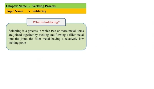
What is BGA BGA is a unique type of surface-mount packaging, which is being used for integrated circuits where electronic components of SMD are actually affixed and mounted on the SMT printed circuit board’s surface. A BGA package usually contains no pins or leads. BGA is featuring leads of ball shape which are being distributed in arrays at the package’s bottom. BGA components have the ability to contain a higher number of pins and larger pitch of the pins. The ball array is actually getting its name because it is a metal or alloy balls array which is arranged in a grid. These balls are usually lead-free. Tin/Silver/Copper or Tin/Lead (Sn/Pb 63/37). BGA packages are being used to mount devices on a permanent basis. It has the ability to provide more interconnection pins which you can put flat or dual in-line packages. However, BGA packages can be assembled on printed circuit boards with the help of SMT applications in a more effective way. https://www.mokotechnology.com/
What is BGA The pins which are being used in this technology are of solder balls which are being arranged in a pattern (usually grid-like pattern) on the package’s undersurface. This is being done to increase the area for connections instead of just periphery. Most interestingly, with BGA soldering, you can get benefits to use the entire bottom surface of the device instead of using perimeter only. However, when it comes to soldering a BGA package in a more successful way requires more précised control and normally done with automated processes. https://www.mokotechnology.com/
What is BGA This is a technique that is being used in the various electronic products to mount different integrated circuits such as FPGAs, WiFi chips and FPGAs, etc. Even more, these packages are also being used in RAM devices, PC Chipsets, and Microcontrollers. https://www.mokotechnology.com/
How does BGA soldering works At the initial stages, the BGA technology was actually a matter of concern. People were not sure about their reliability and soldering. It is because in BGA soldering the pads are normally under the device and are quite invisible. Well, to make sure that you are going on the right path, it is highly important to know the right soldering process. Well, at the present time, the BGA soldering techniques are properly tried and tested to ensure their reliability in the best possible way. However, when it comes to solder BGA packages, then Reflow soldering is the most effective and common technique which is being used for this. https://www.mokotechnology.com/
How does BGA soldering works t is because this can bring the entire PCB assembly to a fixed temperature in order to melt the solder balls which are available under the BGA components. For every BGA soldering, the solder balls are containing a controlled solder amount. When the BGA package and solder balls are being placed in a reflow oven, it will become hot and melt the solder. While the surface tension helps the molten solder in holding the package with right alignment. However, it is highly important to take care of soldering temperature and solder alloy so that it could not melt completely and can manage to stay in semi-solid form. It is also important to keep the solder balls separated from each other to avoid causing any bridging result in the best possible way. https://www.mokotechnology.com/
How does BGA soldering works https://www.mokotechnology.com/
How to inspect BGA solder joints? As it is a well-known fact that SMT and BGA inspection is one of the hardest jobs to handle in a more effectively. It is because inspecting BFGA joints is quite difficult because the solder lies under the BGA package and is invisible. However, the only way in which you can test the BGA solder points satisfactorily is X-rays. It is because X-Rays have the ability to help you to see the joints lying under the BGA package and can provide help in the process of inspection in a more effective way. https://www.mokotechnology.com/
How to inspect BGA solder joints? https://www.mokotechnology.com/
Types of BGA packages Here are some of the most important types of BGA packages which are being used more commonly: 1. MAPBGA MAPBGA stands for “Moulded Array Process Ball Grid Array”. These BGA packages are aiming at the devices ranging from low performance to medium performance for which packaging with ease of surface mounting and low inductance is required. MAPBGA Packages has the ability to provide low-cost solutions with a high level of reliability and a small footprint. 2. PBGA PBGA stands for “Plastic Ball Grid Array”. A package that is designed for the devices ranging from medium to high performance in which ease of surface mounting, low inductance, relatively low cost and maintaining higher levels of reliability is required. This package also contains some extra copper layers which will help in enabling higher levels of power dissipation to be handled. https://www.mokotechnology.com/
Types of BGA packages 3. TBGA TBGA stands for “Tape Ball Grid Array”. This is one of the most common BGA packages which is being used in the applications in which higher thermal performance is required. This BGA package is an effective medium to higher-end solutions for these applications without the use of any external heatsink. 4. TEPBGA TEPBGA stands for “Thermally Enhanced Plastic Ball Grid Array”. This package is capable of providing much higher levels of heat dissipation. In the substrate, thick copper planes are being used to draw heat to the customer board from the die in a more effective way. https://www.mokotechnology.com/
Types of BGA packages 5. MicroBGA As the name of this package is indicating these are the packages which are smaller as compared to the standard BGA packages. There exist 3 different pitches that are predominant in the industry which are 0.65mm, 0.75mm and 0.8mm. 6. PoP PoP stands for “Package on Package”. This type of BGA packages is being used in applications where space is the real concern. It is because this BGA package can allow stacking a memory package on the base package top with ease. To meet a different range of requirements for different types of tools and assembly techniques, these various BGA variants have been developed to make the processes easier and more convenient in the best possible way. https://www.mokotechnology.com/
Advantages of BGA Soldering The Printed Circuit Board which is being used in the electronic gadgets and devices of the present day are compactly populated with multiple electronic components. This is a vital reality with the increase in the quantity of the electronic components on the printed circuit board the size of the circuit board will also increase. However, to squeeze the size of the printed circuit board, BGA and SMDs packages are being used at the present time. It is because both of these packages are slimmer and smaller in sizes and contains a very smaller space on the printed circuit board. However, when it comes to the use of BGA packages in the electronic components of the present time then it is highly important for you to know the benefits which are associated with these packages. Well, here are there major advantages of BGA packages which are important for you to know in this regard. So, have a look at the information given below: https://www.mokotechnology.com/
Advantages of BGA Soldering 1. BGA soldering packages come with High density The BGA is one of the most effective solutions which is designed to resolve the issue of creating a miniature package for an effective integrated circuit containing plenty of pins. Packages of dual-in-line surface mount and Pin grid arrays are being produced with hundreds of pins by decreasing the empty space between these pins. Although this was being used to bring high-density levels, it makes the process of soldering pins was quite difficult to manage. It is because as the space between the pins was decreasing the risk of accidentally bridging head-to-head pins was increasing. However, the BGA soldering packages are a better solution to this problem. https://www.mokotechnology.com/
Advantages of BGA Soldering 2. Heat conduction A more amazing benefit of BGA packages is the decreased thermal resistance between the PCB and the package. This can allow the heat generated inside the package with an integrated circuit for better flow. Even more, it will also prevent the chips from overheating in the best possible way. 3. Lower inductance Well, the shorted electrical conductor means lower inductance. Inductance is a property that has the ability to cause signals’ unwanted distortion in the electronic circuits with high speed. As the BGA contains a short distance between PCB and package, it contains lower lead inductance and will give better performance to the pinned devices. BGA is allowing efficient use of the space of the Printed Circuit Board along with improvement in both electrical and thermal performance. Even more, the decreased package thickness is one of the most amazing benefits which is making this technology more and more popular with every passing day. https://www.mokotechnology.com/
Disadvantages of BGA Technology As with other technologies, BGA is also containing some disadvantages. So, here are the drawbacks of BGA which you must know: 1. BGA inspection requires a complex technique Once the package has been soldered into its place then it would be difficult to find the fault occurring in it. It is because these packages come with a higher level of density which can make it quite difficult to find out the problems. 2. Circuit development is difficult to handle When it comes to the BGA circuit development then it is quite difficult to handle the circuits in a more effective way. BGA packages are more sensitive to the humidity and can cost higher in circuit development. https://www.mokotechnology.com/
Disadvantages of BGA Technology 3. Lack of compliance The most important disadvantage of BGAs is solder balls are unable to flex as the longer leads can. Therefore, these are not complaint mechanically. The predominant use of lead-free solder alloy assemblies is bringing some challenges including “pad cratering” problems, soldering phenomenon and decreased reliability as compared to lead-based solders. However, BGA components are thermal and humidity-sensitive. Therefore, it is always important to store them under constant temperature and in a dry environment. Even more, it is also important for the operators to maintain an effective application environment to avoid any kind of bad effects in the best possible way. However, the optimal storage temperature for BGA components is 20°C- 25°C with a humidity level of less than 10%RH. https://www.mokotechnology.com/
However, for an effective application environment for BGA components, the temperature range should be up to 30°C with a humidity level of less than 60%RH. Most importantly, once the components of the package have been opened then it is important to use them within the duration of 8 hours. MOKO TECHNOLOGY