Download
1 / 15
150 likes | 156 Vues
Technology and its needs are changing on a daily basis, these advancements have led us to the discovery of different great gadgets that made our lives easier than ever.u00a0PCBsu00a0(Printed Circuit Boards) are being used all around the world for their wide range of uses. There are different kinds of PCBs available in the market and they serve different purposes. Heavy Copper PCB is specially designed to work with devices that need high voltages because a normal PCB will not be able to endure this much current.<br>

E N D
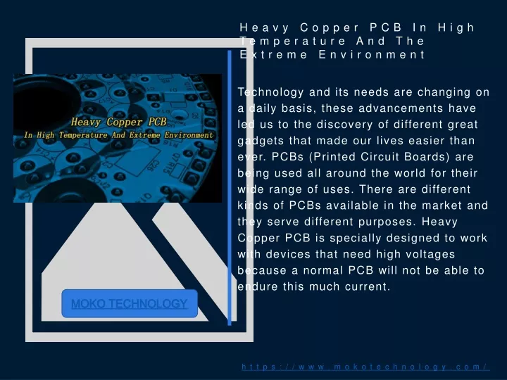
Heavy Copper PCB In High Temperature And The Extreme Environment Technology and its needs are changing on a daily basis, these advancements have led us to the discovery of different great gadgets that made our lives easier than ever. PCBs (Printed Circuit Boards) are being used all around the world for their wide range of uses. There are different kinds of PCBs available in the market and they serve different purposes. Heavy Copper PCB is specially designed to work with devices that need high voltages because a normal PCB will not be able to endure this much current. MOKO TECHNOLOGY https://www.mokotechnology.com/
Heavy copper PCB in high temperature and extreme environment It is always a good idea to consider all sides of a product before you use it. So, is heavy copper PCB good in high temperatures and the extreme environment? Well, yes! They can perform well in extreme weather and high temperature as well. A lot of companies have been using the heavy copper PCB in their products because of their working in extreme weather. How much current on a heavy copper circuit board can be transported? This question usually depends on the design of electronics. The thickness and width of copper and heavy copper printed circuit boards at maximum temperature include bearing capacity. This question arises because the heat generated by heavy copper printed circuit boards during operation is closely related to current. 1 3 4 https://www.mokotechnology.com/
Heavy copper PCB in high temperature and extreme environment When current flows through wires, the average power consumption during operation is 12% of the initial energy, so locally lost energy generates heat transfer, which will be dissipated in the environment as a heat conductor. The wires with the maximum current must be found on heavy copper printed circuit boards, a method for evaluating the temperature increase, and the corresponding exposure current should be found. https://www.mokotechnology.com/
Heavy copper PCB in high temperature and extreme environment How much current on a heavy copper circuit board can be transported? This question usually depends on the design of electronics. The thickness and width of copper and heavy copper printed circuit boards at maximum temperature include bearing capacity. This question arises because the heat generated by heavy copper printed circuit boards during operation is closely related to current. https://www.mokotechnology.com/
Heavy copper PCB in high temperature and extreme environment When current flows through wires, the average power consumption during operation is 12% of the initial energy, so locally lost energy generates heat transfer, which will be dissipated in the environment as a heat conductor. The wires with the maximum current must be found on heavy copper printed circuit boards, a method for evaluating the temperature increase, and the corresponding exposure current should be found. https://www.mokotechnology.com/
Heavy copper PCB in high temperature and extreme environment PCB manufacturers and developers are offered a variety of materials, ranging from high-quality substrates, from conventional FR-4 epoxy backing materials with a working temperature of 130 ° C to high-temperature Tg materials. A series of ways have been developed to test the heat resistance of end products containing PCBs. Because of the change in thermal expansion between the copper and the substrate, a “driving force” is created between them, and this means thermal stress, which can lead to cracking, trapping, and growth, which ultimately leads to failure of the printed circuit board. https://www.mokotechnology.com/
Heavy copper PCB in high temperature and extreme environment In the rotation test for nozzle ability during thermal shock control, a group of 32 series-coated nozzles is designed as a sample on the map, and their condition will be checked after the thermal shock test. The first coating defect during the hole will be determined based on the thermal pressure that the circuit board can withstand. The use of heavy copper printed circuit boards in the heatstroke cycle will reduce or eliminate malfunctions. https://www.mokotechnology.com/
The benefits of heavy copper PCB fabrication The main reason to choose something is the number of advantages they provide and their wide range of uses. Well, thick copper PCB offers a number of uses and benefits that make our life easier and products better. We have listed a number of benefits below: Higher resistance to thermal stress An increase in the current load Increased mechanical strength at conductor sites and PTH holes Usage of exotic materials to their full potential (i.e., at high temperature) without interrupting the circuit Reduce the size of the product by incorporating several weights of copper in the same circular layer Heavy copper panels carry higher current through the plate and help transfer heat to the external heat sink The cold rooms are directly integrated into the surface of the plate using copper tops up to 120 ounces High power density on-board transformers https://www.mokotechnology.com/
Copper thickness of heavy copper PCB Board Heavy copper means the foil thickness of the Printed Circuit Board greater than 3 oz (100 microns or four mils) typically. It is usually used for high electric current supply or some power circuits that are used in the automotive business. It can also be designed in the outer layer or inner layer. The thickness of heavy copper can also vary depending on the manufacturer, but they offer the same purpose. You should always use the best heavy copper PCB with the right thickness because a poor PCB cannot pass the heavy current. So, using a poor quality PCB leads to the failure of your product. Consider heavy copper PCB thickness an important factor because you shouldn’t leave anything on chances. There are a lot of companies that are making the heavy copper PCB that can be used to fulfill all of your requirements. https://www.mokotechnology.com/
Main heavy copper PCB specification to be considered In the making of printed circuit boards for thick copper printed circuit boards or heavy copper printed circuit boards, people usually use this name to designate a printed circuit board with a copper thickness of greater than 3 ounces in the inner or outer layers. And a very heavy copper printed circuit board indicates a printed circuit board of more than 15 ounces. Thick copper plate technology allows complex switches to be implemented in narrow spaces in combination with high current circuits. The multilayer circuit board has reliable processes for producing a copper layer up to 20 ounces thick. Copper printed circuit board is usually used in high power rectifiers, in computers, for charging electric vehicles, in electrical network switching systems, etc. https://www.mokotechnology.com/
Thick Copper Design Guide Like standard FR4 printed circuit boards, heavy copper printed circuit boards have the same manufacturing method with unique engraving and coating technologies such as high-speed ink drilling and deviation engraving. Some time ago, people tried to make heavy copper printed circuit boards with a minimal pattern. Some printed circuit boards made in this way have been damaged by scrap due to uneven edge lines and excessive drilling. To avoid this, advanced painting and engraving techniques have been applied so that direct edge engraving and perfect edges can be obtained. The coating on a copper PCB allows PCB manufacturers to increase both the covered wall and the wall with benefits that include: https://www.mokotechnology.com/
Thick Copper Design Guide Impedance distribution reduction Manufacturing costs reduction Layer count shrinking Packaging minimization The heavy copper printed circuit board can easily be connected to an ordinary printed circuit board. As for the tracing, the smallest distance between a printed circuit board and a range in its tolerance and production capacities, it must be defined by a discussion between the design engineers and the manufacturers before the actual manufacturing https://www.mokotechnology.com/
Applications Of Heavy Copper PCB Boards The printed circuit board or PCB is a mixture of plating and etching on copper. The circles used in the process are layers and etched to remove unwanted copper. It is plated to add the thickness of copper to planes, rails, cushions, and through holes. These chain layers are laminated with epoxy-based support such as FR4 or Polyimide. Heavy copper PCB has an integrated core of base metals. The heavy PCP core helps dissipate heat and radiate various components of the plates. This PCB does not apply for all purposes, but to meet the particular needs of customers. They are used in industry for applications such as welding equipment, the solar cell manufacturing process, power supply, the automotive industry, electrical distribution, and power transformers. https://www.mokotechnology.com/
Applications Of Heavy Copper PCB Boards This helps dissipate heat and reduces its base temperature. This application protects the device itself from damage. It can transfer heat from the component at a much higher speed. This is a high-frequency PCB limited to those that cannot be cooled using traditional fan cooling technology. The plates laminate spread and dissipate heat, which makes the device much colder and, thus, increases the performance of the devices and increases their productivity. The heavy copper circuit board is made from a mixture of various special alloys. Copper PCBs are also rated 8–9 times faster than modern PCBs. It is also useful for recording the performance of LED devices and for preventing bumps. When using LED devices, high-density copper printed circuit boards must be used. https://www.mokotechnology.com/
Working with MOKO Technology for your thick copper PCB Reliable operation and excellent temperature control are the main factors in determining the demand for copper printed circuit boards. Today’s circuits are designed to pass a strong current, which means that a lot of heat is generated. However, heavy copper circuits boards will help dissipate heat efficiently, thus ensuring optimal circuit performance. If you are still unsure of the technical problem of copper circuit boards in your electrical applications, you can always contact an electrical engineering specialist or a reliable manufacturer of heavy copper circuit boards. MOKO Technology can help you with your PCBs need. MOKO TECHNOLOGY