Download
1 / 111
1.16k likes | 1.69k Vues
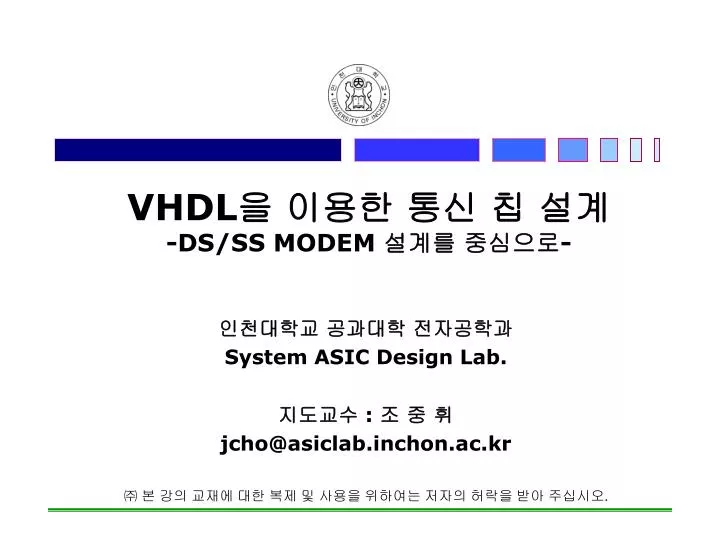
VHDL 을 이용한 통신 칩 설계 -DS/SS MODEM 설계를 중심으로 -. 인천대학교 공과대학 전자공학과 System ASIC Design Lab. 지도교수 : 조 중 휘 jcho@asiclab.inchon.ac.kr ㈜ 본 강의 교재에 대한 복제 및 사용을 위하여는 저자의 허락을 받아 주십시오. 단계별 구성 시스템 이해 알고리즘 설계 RTL 블록 설계 VHDL 표현 검증 및 합성 FPGA Emulation Physical 설계 ASIC 으로의 제작 System Board 구성

E N D
VHDL을 이용한 통신 칩 설계 -DS/SS MODEM 설계를 중심으로- 인천대학교 공과대학 전자공학과 System ASIC Design Lab. 지도교수 : 조 중 휘 jcho@asiclab.inchon.ac.kr ㈜ 본 강의 교재에 대한 복제 및 사용을 위하여는 저자의 허락을 받아 주십시오.
단계별 구성 시스템 이해 알고리즘 설계 RTL 블록 설계 VHDL 표현 검증 및 합성 FPGA Emulation Physical 설계 ASIC으로의 제작 System Board 구성 ASIC의 검증 ASIC 선택 FPGA SOG Cell-Based Full Custom ASIC 제품의 기획, 설계 및 구현 과정에 대한 기본 이해
설계 대상체의 동작 및 구조 특성에 대한 표현의 다양성 • 설계 사양의 표현 수준 • System Level • Behavioral Level • RTL Level • Logic Level • Circuit Level • Layout Level • 설계 사양의 표현 • Graphic Diagram • HDL 표현 • 설계 단계에 대한 이해
Synthesis 가능한 VHDL 표현을 위한 Hardware 추출 • Target Architecture • Register-Transfer Level의 블록 구성도 • RTL 회로도의 주요 구성 요소 • 조합 논리 회로 블록 : Basic Gates, Modular Units (mux, decoder, arithmetic units) • 동기 신호 요구 블록 : F/Fs, Registers • 기억 소자 블록 : ROM, RAM • Bus 연결 요구 블록 : 3-Buffer
Design Flow의 3단계 구성과 의미 RTL 회로 설계 회로도 추출 및 효율적 VHDL 표현 기능 Simulation에 의한 회로 검증 Gate Level 회로 설계 면적,속도,Power를 고려한 조건 설정 Design Library의 설정 : FPGA, ASIC Component Delay를 고려한 기능 및Timing Simulation에 의한 회로 검증 Physical Design을 위한 EDIF 생성 FPGA를 이용한 Physical Design FPGA Tool에 의한 Compile 수행 사용할 Device 및 Option의 설정 Layout Data를 이용한 Simulation Target Board의 구성과 Emulation을 통한 검증 ASIC으로의 변환 여부에 따른 대응 ASIC 설계를 위한 Physical Design Design House와의 연계 및 EDIF 전달 Wire Delay를 함께 고려한 Simulation Sign-off 와 ASIC에 대한 기다림 Test Board 구성, 검증 및 평가 Design Flow의 모형 VHDL 표현과 Design Compiler에 의한 설계
다양한 Digital ASIC 구현 방법 • Digital ASIC 구현의 종류
Digital ASIC 구현 방법에 대한 선택 • 응용과 시장성을 고려한 ASIC 제품의 특성 비교
Standard-Cell Design에 대한 개념 • Boding Diagram 예제
Sea-of-Gate Design에 대한 개념 • Boding Diagram 예제: FLEX Decoder Chip
HDL의 비교 및 VHDL의 변화 과정 • 표준화를 목표로 하면서 사용되고 있는 HDL 의 비교 • VHDL : 시스템에 대한 기술의 능력은 매우 높으나, synthesis를 위하여 sub-set VHDL과 modeling에 대한 guide가 요구. • Verilog : VHDL보다는 기술의 능력이 높지는 않으나 널리 사용되고 있으며, gate 레벨의 simulation 언어로는 매우 적합하여 design kit의 golden simulator에 사용 • VHDL의 개발과 변화 • Value 체계에 대한 변화 • 1987년의 STD-1076 Version • STD library에 정의된 2-Value 체계 즉, {‘0’, ‘1’}를 기본으로 사용 • 1990년을 전후로 하여 Value 체계에 대한 표준안에 대한 요구 • IEEE library에 정의된 9-value 체계 즉, {‘U’, ‘X’, ‘0’, ‘1’, ‘Z’, ‘W’, ‘L’, ‘H’, ‘-’}를 사용
VHDL의 다양한 사용 목적 • 사용 관점에 따른 목적의 다양성 • System 설계자의 관점 : Simulation과 Documentation • Chip 설계자의 관점 : Simulation, Synthesis 및 Documentation • Chip 설계자에의 유용성 및 제약성 • IP(Intellectual Property) Model에 대한 개발과 Re-Use의 개념이 가능 • Synthesis가 가능한 VHDL 표현과 효율적인 Modeling 방법의 이해가 요구
H/W 및 S/W 관점에서 요구되는 Interface 와 Body의 2가지 개념 • VHDL을 이용한 표현의 단위를 Design Entity라 부름 • 표현하고자 하는 hardware design 대상체를 의미함 • 예시 : NOT gate, ALU, Micro-Processor, Board, Computer System 등 • VHDL에서 Design Entity를 표현하기 위하여 요구되는 개념
System 분할과 VHDL 표현을 위한 개념(1) • System에 대한 분할을 위한 개념 • System 개념 또는 설계자가 이해할 수 있는 범위에 따른 분할함 • IP 또는 Macro Component로 구성되어 있는 경우의 분할함 • 논리 합성의 대상체는 4,000~5,000 Gate가 Optimization 관점에서 보편적으로 적합함 • 분할에 대한 표현 예-1 • Design Tree와 Fully 계층적VHDL 표현 • 모든 Design Node를 Entity Unit + Architecture Unit으로 표현 • 논리 합성의 결과는 계층적으로 나타나므로 분할의 정보를 유지함
System 분할과 VHDL 표현을 위한 개념(2) • 분할에 대한 표현 예-2 • Design Tree와 Fully Flatten VHDL 표현 • Root Design Node에 대하여 만 Entity Unit + Architecture Unit으로 표현 • Root 이외의 Design Node는 Concurrent VHDL 구문을 사용하여 표현 • 논리합성의 결과는 하나의 도면으로 나타나므로 분할의 정보가 유지되지 않음 • 분할에 대한 표현의 다양성 • 위의 2가지 표현 사이에 여러 가지 다양한 표현이 가능함 -> 설계자의 선택 사항
Entity Declaration Unit의 정의 • Entity Unit에 대한 기본 개념의 표현 • Entity Unit 표현에 대한 Syntax 정의 entity ENTITY_NAME is [ generic( LIST_OF_GENERICS_AND_THEIR_TYPES ) ; ] [ port( LIST_OF_PORTS_AND_THEIR_MODE ) ; ] [ DECLARATIONS ] [ begin { ENTITY_STATEMENT } ] end [ entity ] [ ENTITY_NAME ] ;
D Flip-Flop의 Symbol Entity Unit의 설계 -- 9-value Package 공유를 위한 Visibility library IEEE; use IEEE.std_logic_1164.ALL; -- Pin Name, Mode, Data Type의 표현 entity DFF is port (D : in std_logic; CLK : in std_logic; CLR : in std_logic; -- D, CLK, CLR : in std_logic; Q, QBAR : out std_logic); end DFF; Generic Decoder의 Symbol Entity Unit의 설계 library IEEE; use IEEE.std_logic_1164.ALL; entity GENERIC_DECODER is -- Static Information에 대한 표현 generic (SIZEIN, SIZEOUT : integer); -- Dynamic Pin Data에 대한 표현 port (EN: in std_logic; A : in std_logic_vector (SIZEIN-1 downto 0); B : out std_logic_vector (SIZEOUT-1 downto 0)); end GENERIC_DECODER; Entity Declaration Unit의 예제
Architecture Unit에 대한 개념과 표현 형태 • 예제 회로에 대한 이해의 관점에 대한 분류 • behavioral view • Q=‘1’이기 위한 조건은 x=‘1’ 이거나, Y와 Z가 동시에 ‘1’인 경우라 분석하여 순서적으로 수행되는 구문을 사용하여 동작적 특성을 기술하는 관점이다. • data-flow view • Boolean 또는 state equation의 형태로 분석하여 동시적으로 수행되는 구문을 사용하여 동작적 특성을 기술하는 관점이다. • structural view • and gate와 or gate의 연결에 의한 구성으로 분석하여 구조적 특성을 기술하는 관점이다. 이때 and 및 or gate는 위의 2가지 중 하나로 표현되어야 한다. • mixed view • 위의 3가지가 혼합되어 사용되는 표현
Entity design unit library IEEE; use IEEE.std_logic_1164.all; entity EXAMPLE is port (X, Y, Z: in std_logic; Q: out std_logic); end EXAMPLE; Behavioral architecture body unit architecture RTL1 of EXAMPLE is begin process (X, Y, Z) begin if X=‘1’ then Q <= ‘1’; elsif (Y=‘1’ and Z=‘1’) then Q <= ‘1’; else Q <= ‘0’; end if; end process; end RTL1; Data-flow architecture body unit architecture RTL2 of EXAMPLE is begin Q <= X or (Y AND Z); end RTL2; Structural architecture body unit architecture RTL3 of EXAMPLE is component OR2 port (I1, I2: in std_logic; O1: out std_logic); end component; component AND2 port (I1, I2: in std_logic; O1: out std_logic); end component; for U0: OR2 use entity work.OR2(RTL); for U1: AND2 use entity work.AND2(RTL); signal S1: std_logic; begin U0: OR2 port map (X, S1, Q); U1: AND2 port map (Y, Z, S1); end RTL3; Architecture Body Unit에 대한 다양한 표현 형태
Source file과 Compiled file의 관계 • VDHL source file을 compile하는 경우 • library의 지정이 요구되며, compiled file (intermediate format)은 지정된 library에 저장 • WORK library에 대한 개념 정의 • VHDL 사용자가 사용하고 있는 현재의 library를 편의상 WORK로 부르기로 약속함 • IEEE VHDL 표준화 위원회(VASG)에서 지정한 library • 2-value를 위한 STD 와 9-value를 위한 IEEE • VHDL Analyzer에 의한 처리 과정
Library의 종류와 Visibility의 범위 • Library의 종류 • VHDL Code에서 Package Unit을 사용하기 위한 Visibility의 부여 방법 • 공유하는 package가 WORK library에 있는 경우 design unit의 기술 앞에 다음을 기술 • use WORK.package_name.item_name; • 공유하는 package가 예를 들어 LIB1인 경우 design unit의 기술 앞에 다음을 기술 • library LIB1; use LIB1.package_name.item_name;
Library Visibility의 표현과 영향의 범위 • Entity Unit의 표현 앞에 기술하는 경우 • 해당되는 architecture와 configuration unit까지만 영향을 받음 --library visibility의 부여 library IEEE; use IEEE.std_logic_1164.ALL;use IEEE.std_logic_unsigned.all; --entity unit에 대한 표현 시작 entity ADD_SUB is port ( A, B : in std_logic_vector(3 downto 0); SEL : in std_logic; S : out std_logic_vector(3 downto 0); CF, ZF : out std_logic); end ADD_SUB; • Package Declaration Unit의 표현 앞에 기술하는 경우 • 해당되는 package body unit까지만 영향을 받음 library IEEE;use IEEE.std_logic_1164.ALL; use IEEE.std_logic_arith.all; use IEEE.std_logic_signed.all; package PACK_MATCH is function COMP2C ( A: std_logic_vector) return std_logic_vector; function TWO_MUL ( A: std_logic_vector; B: std_logic) return std_logic_vector; end PACK_MATCH;
Structural View의 표현을 위한 기본 개념의 정의 • Schematic Capture System과 VHDL 표현과의 비교 • Capture System에서 사용하는 Component에 대한 선택 • Architecture Unit에 Component로 선언하며, 특정 Component로 지정 • Symbol Edit 또는 Copy 기능에 의하여 회로 구성 • Component Instantiation 구문에 의하여 회로 구성 • 회로 구성 시에 요구되는 Wire의 사용 • Wire는 Signal Object로 선언하고 사용 • Formal Name 과 Actual Name에 대한 정의 • Formal Name : 선언된 Component의 Generic 및 Port Name으로 Pin Name을 의미함 • Actual Name : Hardware 구현 시의 Generic 및 Port Name으로 Wire Name을 의미함 • 표현을 위한 3가지 형태의 구문 • Component Instantiation 구문, For..Generate 구문, IF.. Generate 구문 • 예제 회로 : 1-Bit Half-Adder와 등가 회로
Formal Name과 Actual Name을 연결하는 2가지 방법 Positional Association Mapping Named Association Mapping 앞의 회로에 대한 VHDL 표현 library IEEE; use IEEE.std_logic_1164.all; entity HA is port (X, Y : in std_logic; S, C : out std_logic); end HA; architecture RTL of HA is --Component의 Formal Name 선언 component NAND2 port ( A, B : in std_logic; Y : out std_logic); end component; component INV port ( X : in std_logic; Y : out std_logic); end component; -- 2 종류의 Component의 Link 정보 표현 for U4 : INV use entity work.INV(RTL); for others: NAND2 use entity work.NAND2(RTL); -- 연결 Wire에 대한 Data Object 선언 signal S1, S2, S3 : std_logic; begin -- Positional Association Mapping 예제 U0 : NAND2 port map (X, Y, S3); U1 : NAND2 port map (X, S3, S1); U4 : INV port map (S3, C); -- Named Association Mapping 예제 U2 : NAND2 port map (A => S3, Y => S2, B => Y); U3 : NAND2 port map (A => S1, B => S2, C => S); end RTL; 사용되는 Component에 대한 VHDL Modeling은 미리 Compile 되어 지정 Library에 저장하여야 한다. Component Instantiation 구문에 의한 표현
Unconnected Port에 대한 정의 Actual Name이 존재하지 않는 경우 Unconnected Output Port Unconnected Input Port Unconnected Port에 대한 회로 예제 Unconnected Input Port VCC를 ‘1’로 정의하고 연결함 Unconnected Output Port Reserved Identifier인 OPEN을 연결함 Unconnected Port에 대한 처리 예제 architecture RTL of EX1 is component EX2 port (CLK, PRESET, RESET, D : in std_logic; Q, QBAR : out std_logic); end component; for U1: EX2 use entity work.DFFSR(RTL); signal VCC : std_logic; begin -- VHDL-87에서의 처리 방법 VCC <= ‘1’; U1 : EX2 port map (D => D, CLK =>CLK, PRESET =>VCC, RESET=>CLR, Q=>Q,BAR=>open); -- VHDL-93에서의 처리 방법 U1 : EX2 port map (D => D, CLK=>CLK, PRESET =>’1’, RESET=>CLR, Q=>Q, QBAR=>open); end RTL; Unconnected Port에 대한 처리 방법
Generic 구문의 Behavioral 표현 entity AND_GATE is generic (Tdelay : time := 10 ns; N : positive := 2); port (A : in std_logic_vector(N-1 downto 0); C : out std_logic); end AND_GATE; architecture RTL of AND_GATE is begin P0 : process (A) variable INT : std_logic; begin INT := ‘1; for I in (A’length-1) downto 0 loop if (A(I)=‘0’) then INT := ‘0’; end if; end loop; C <= INT after Tdelay; end process; end RTL; Generic Map을 갖는 Structural 표현 entity EX is port (D1, D2, D3, D4, D5 : in std_logic; Q1, Q2 : out std_logic); end EX; architecture RTL of EX is component AND_COMP generic (TDELAY : time; N : positive); port (A : in std_logic_vector(N-1 downto 0); C : out std_logic); end component; for all : AND_COMP use entity work.AND_GATE(RTL); begin U1: AND_COMP generic map (n=>2, TDELAY=>8 ns) port map (A(0)=>D1, A(1)=>D2, C=>Q1); U2: AND_COMP generic map (n=>3, TDELAY=>12 ns) port map (A(0)=>D3, A(1)=>D4, A(2)=>D5, C=>Q2); end RTL; Generic Map Command의 사용
Behavioral View의 표현을 위한 구문 • 병렬적인 수행을 행하도록 정의된 구문 • basic signal assignment statement • conditional signal assignment statement • selected signal assignment statement • process statement with many sequential statements • concurrent subprogram call statement • block statement with guarded signal assignment statement • concurrent assert statement • 순서적인 수행을 행하도록 정의되 구문 • process 구문, function 또는 procedure와 같은 subprogram 내에서만 사용 • basic signal assignment statement • variable assignment statement • if statement • case statement • loop statements : for..loop statement, while loop statement, infinite loop statement • next statement, exit statement • null statement • sequential subprogram call statement • wait statement • sequential assert statement
Full-Adder 회로와 각 Gate에 대한 Sensitivity Signal에 대한 개념 정의 Basic Signal Assignment 구문에 의한 Architecture Unit의 설계 architecture RTL of ADDER is signal S0, S1 : std_logic; begin --각 gate를 signal assignment 구문으로 표현 S0 <= A xor B; S1 <= A and B; SUM <= S0 xor CIN; COUT <= S1 or (S0 and CIN); end RTL; 다양한 형태의 Signal Assignment 구문 Aggregate : 하나의 Target Signal에 여러 개로부터의 Source 값을 Assign 하는 경우 architecture RTL of EX is signal A : std_logic_vector( 4 downto 0); signal B : std_logic_vector( 4 downto 0); begin A <= (others => ‘0’); -- A <= “00000”; -- A <= (‘0’, ‘0’, ‘0’, ‘0’, ‘0’); B <= (1=>C(2), 3=>C(1), others => D(0)); -- B <= D(0)&C(1)&D(0)&C(2)&D(0); end RTL; 하나의 Source 값을 여러 개의 Target Signal에 나누는 경우의 표현 방법에 대하여도 생각하여 보자. Basic Signal Assignment 구문 예제
Conditional Signal Assignment 구문의 정의와 예제 • Syntax 정의와 동작 개념 signal_identifier <= waveform_1 when condition_1 else waveform_2 when condition_2 else ……………… waveform_(N-1) when condition_(N-1) else waveform_N ; • D Type Flip-Flop의 VHDL 표현과 Symbol architecture A2 of DFF is begin Q <= ‘0’ when CLR=‘0’ else D when (CLK=‘0’ and CLK’EVENT) else Q; QBAR <= not Q; end A2; • Data Selector에 대하여 Conditional Signal Assignment 구문에 의한 표현 MUXOUT <= I0 when (SEL=‘0’) else I1;
Syntax 정의와 동작 개념 with expression select signal_identifier <= waveform1 when expression_1, ………………... waveform(n-1) when expression(n-1), waveform(n) when others ; 1-Bit Half-Adder에 대한 표현 library IEEE; use IEEE.std_logic_1164.ALL; entity HA is port (A, B : in std_logic; SUM, COUT : out std_logic); end HA; architecture RTL of HA is signal TMP1, TMP2 : std_logic_vector(1 downto 0); begin TMP1 <= A & B; with TMP1 select TMP2 <= “00” when “00”, “01” when “01”, “01” when “10”, “10” when others; (COUT, SUM) <= TMP2; end RTL; 2*1 MUX에 대한 표현 library IEEE; use IEEE.std_logic_1164.ALL; entity MUX21 is port (SEL, A, B : in std_logic; C : out std_logic); end MUX21; architecture RTL of MUX21 is begin with SEL select C <= A after 10 ns when ‘0’, B after 10 ns when others; end RTL; Selected Signal Assignment 구문의 정의와 예제
Syntax 정의 [ Label : ] process [ ( Sensitivity_Signals ) ] -- declaration statements begin -- sequential activity statements end process [ Label ] ; 동작 개념 Sensitivity Signal List가 있는 경우 Wait 구문을 포함할 수 없다. Simulation에 대한 수행 명령과 함께 각 Signal의 초기값을 갖고 내부 구문에 대한 1회의 수행을 수행한다. 수행 완료와 함께 Process 문에 표현된 Sensitivity Signal List에 포함된 Signal 중 어느 하나라도 Event가 생기는 가를 검사하여 Event가 발생하면 Process 문에 대한 Simulation을 다시 수행한다. 합성 H/W 표현에 이용 권장 Sensitivity Signal List가 없는 경우 적어도 1개 이상의 Wait 구문을 포함해야 한다. Simulation의 시작과 함께 Wait 구문을 만날 때까지의 구문을 수행한다. Wait 구문을 만나면 해당 조건을 만족할 때까지는 Simulation을 중지한다. Stimulus Vector 표현의 이용 권장 AND Gate에 대한 표현 process (A, B) begin C <= A and B; end process; Sensitivity Signal이 차이에 따른 문제점 이해 A, B를 모두 기술한 경우 A만 기술한 경우 Process 구문에 대한 정의와 예제
If 구문에 대한 정의와 사용 예제 • Syntax 정의와 동작 개념 • if ... then … end if; (주의 사항: Latch 생성 요인이 있음) • if ... then ... else … end if; • Nested if Statements • 다음의 Architecture Unit으로부터 생성되는 파형을 예측하여 보자. architecture RTL of OSC is signal CLK : std_logic := ‘0; begin process variable SWITCH : std_logic := ‘0’; begin if SWITCH=‘0’ then CLK <= ‘0’; else CLK <= ‘1’; end if; SWITCH := NOT SWITCH; wait for 25 ns; end process; end RTL;
Syntax 정의와 동작 개념 case EXPRESSION is when EXPRESSION_VALUE_1 => (sequential_statements;) ….. when EXPRESSION_VALUE_(N-1) => (sequential_statements;) whenothers => (sequential_statements;) end case ; Truth Table에 대한 표현에 적합함 1-Bit Half-Adder에 대한 표현-1 architecture RTL1 of EX is begin process (A, B) variable TMP1, TMP2 : std_logic_vector(1 downto 0); begin TMP1 := A & B; case TMP1 is when “00” => TMP2 := “00”; when “01” | “10” => TMP2 := “01”; when others => TMP2 := “10”; end case; (COUT, SUM) <= TMP2; end process; end RTL; 1-Bit Half-Adder에 대한 표현-2 Signal에 Over-Writing 하는 경우 의미 architecture RTL2 of EX is begin p1: process (A, B) variable TMP: std_logic_vector(1 downto 0); begin TMP := A & B; (COUT, SUM) <= “00”; case TMP is when “00” => null; when “01”|”10” => SUM<= ‘1’; when others => COUT <= ‘1’; end case; end process; end RTL2; Case 구문에 대한 정의와 사용 예제
For..Loop 구문의 Syntax [Label:] for loop_parameter in discrete_range loop --sequential statements end loop [Label]; VHDL 표현 예제-1 process (A) variable sum : signed(7 downto 0); begin sum := (others => ‘0’); for I in 7 downto 0 loop sum := sum + A(I); end loop; sum_out <= sum; end process; 예제-1에 대응하는 Flow-Graph을 생각하여 보자. 동작 속도의 관점에서 효율적인 VHDL 표현을 생각하여 보자. VHDL 표현 예제-2 process (A) variable count : integer; begin count := 8; for LEVEL in 0 to 2 loop count := count / 2; for I in 0 to (count-1) loop A(I) := A(I*2) + A(I*2+1); end loop; end loop; sum_out <= A(0); end process; discrete_range 표현 방법 integer_expression TO integer_expression integer_expression DOWNTO integer_expression array_attribute’RANGE array_attribute’REVERSE_RANGE For..Loop 구문에 대한 정의와 사용 예제
Next 구문의 Syntax와 개념 next; next loop_label; next when boolean_expression; next loop_label when boolean_expression; 예제 LBL1 : process (S) variable TMP, J : integer := 0; begin TMP := 0; J := 0; A_LOOP: for I in 0 to 7 loop J := J + 1; if I > 5 then next A_LOOP; end if; TMP := TMP + 1; end loop; end process LBL1; Exit 구문의 Syntax와 개념 exit; exit loop_label; exit when boolean_expression; exit loop_label when boolean_expression; 예제 LBL2 : process (S) variable SUM, CNT : integer := 0; begin SUM:= 0; CNT:= 0; FIRST: loop CNT:=CNT+1; SUM:=SUM+CNT; exit when SUM > 100; end loop FIRST; SECOND: loop CNT:=CNT+1; SUM:=SUM+CNT; if SUM > 100 then exit; end loop SECOND; end process LBL2; Next와 Exit 구문에 대한 정의와 사용 예제
VHDL의 Test Bench Modeling의 개념 • Test Harness를 위한 기본 구조 • Synthesis를 목적으로 표현된 Hardware VHDL Model • Simulation을 위한 입력 Data를 생성하는 Vector Generation VHDL Model • Test Harness 내부에서 생성 • Array에 상수 형태로 저장된 Vector를 읽으면서 수행 • 별도의 System File에 저장된 Vector를 읽으면서 수행 • Simulation Tool에 의한 계산 값과 설계자의 기대 값을 비교하는 VHDL Model • 출력된 파형에 대하여 설계자가 추적하여 Simulation 결과를 판단하는 방식 • Simulation 결과를 File로 출력하는 방식 • 기대 값과 계산 값을 assert 구문을 비교하여 Pass/Fail 만을 출력하는 방식 HDL Test Harness MODEL UNDER TEST One, or possibly more component instantiation(s) Stimulus Output of hardware model under vectors vectors test. WAVEFORM Results COMPONENT RESULTS Test File GENERATON Compare and possibly Vectors (may include other parts generate pass /fail Reference vectors of modeled hardware File Pass/fail indication. system) indication
Test Vector 생성에 대한 3가지 모형과 VHDL 표현 • Case1 : 초기화 신호 및 반복적 특성의 Clock 신호 생성 • case2 : Random하게 변화하는 신호의 생성 (1개의 구문 사용) • case3 : Random하게 변화하는 신호의 생성 (여러 개의 구문 사용)
--9-value visibility 부여 library IEEE; use IEEE.std_logic_1164.ALL; --entity unit에 대한 표현 entity TB is port (CLOCK1 : buffer std_logic := ‘0’; CLOCK2, RESET1, RESET2 : out std_logic ; ENABLE : out std_logic; A_DATA, B_DATA : out std_logic_vector(7 downto 0)); end TB; --architecture unit에 대한 표현 architecture TB_A of TB is begin CLOCK1 <= not CLOCK1 after 20 ns; RESET1 <= ‘0’, '1' after 100 ns; process begin if now = 0 ns then CLOCK2 <= '0'; wait for 250 ns; else CLOCK2 <= '1'; wait for 20 ns; CLOCK2 <= '0'; wait for 20 ns; end if; end process; process begin A_DATA <= "00101101"; B_DATA <= "10110110"; wait for 120 ns; A_DATA <= "11011011"; wait for 30 ns; B_DATA <= "00001010"; wait for 90 ns; A_DATA <= "00011011"; wait for 150 ns; end process; process begin if now = 0 ns then RESET2 <= '0'; ENABLE <= '0'; wait for 50 ns; else RESET2 <= '1'; ENABLE <= '1'; wait for 300 ns; ENABLE <= '0' after 200 ns, '1' after 400 ns; wait for 800 ns; RESET2 <= '0', '1' after 150 ns; ENABLE <= '0' after 50 ns; wait for 200 ns; end if; end process; end TB_A; Test Vector 생성을 위한 Modeling 예제
Test Vector 생성 Waveform과 의미 분석 • Test Vector 생성을 표현하는 Waveform • 생성 신호에 대한 의미 분석 • CLOCK1, CLOCK2와 같이 주기성을 갖는 신호 • RESET1, RESET2와 같이 변화의 빈도가 매우 적은 특징을 갖는 신호 • A_DATA, B_DATA와 같이 변화의 빈도가 많은 특징을 갖는 신호 • 보편적인 제어 신호와 Data 신호가 해당 • Process 구문을 사용한 표현이 적합함
Spread Spectrum 통신 시스템에 대한 개념도 • 주요 구성부 • Source CODEC • Channel CODEC • Modulator-Demodulator
Direct-Sequence Spread-Spectrum 시스템 • DS/SS System에 대한 블록 구성도 • PN Sequence에 대한 이해 • 주기가 15인 PN Sequence에 대한 예 • PN 신호의 자기 상관 함수 성질에 대한 이해
Frequency-Hopping Spread-Spectrum 시스템 • FH/SS System에 대한 블록 구성도
DS/SS-BPSK 송신부 구조와 동작에 대한 이해 • 기본 블록 구성과 신호 예제
DS/SS-BPSK 수신부 구조와 동작에 대한 이해 • 기본 블록 구성과 신호 예제
DS/SS-QPSK 송신부와 수신부의 기본 구조 • 송신부에 대한 기본 블록 구성 • 수신부에 대한 기본 블록 구성
DS/SS-QPSK 송신부의 신호 예제를 통한 동작 이해 • 신호 예제
Differential BPSK 송신부의 기본 구조 • Differential BPSK (DBPSK) Modulator의 기본 구조 • 동작에 대한 이해 • 현재의 심벌과 이전 심벌간의 논리 회로의 결과를 출력한다. • 이전 심벌은 지연 소자(Register)를 사용하여 기억한다. • 한 심볼 구간(Tb)을 지연 시킨 Register의 출력은 Feedback 한다. • 논리 회로는 XOR나 XNOR를 사용하는데, 현재의 심벌과 이전 심벌간의 위상의 합은 XOR로 구현한다. • Level shift block은 차동 부호화된 심볼(‘0’ or ‘1’)을 부호 확장하여 ‘1’ or ‘-1’로 변환하는 블록이다. • 차동 부호화된 심벌에 반송 주파수(carrier Frequency)를 곱하여 BPSK(Binary Phase-Shift-Keying)를 하고 대역 통과 필터(band Pass Filter)를 취한다. • 수신부에서 Non-Coherent 시스템을 사용하는 경우 수신부 구조의 간결화 가능
Differential BPSK 수신부의 2가지 형태의 구조 • Differential BPSK (DBPSK) Demodulator • non-coherent detection • Differentially Encoded BPSK(DEBPSK) Demodulator • coherent detection