Download
1 / 32
320 likes | 399 Vues
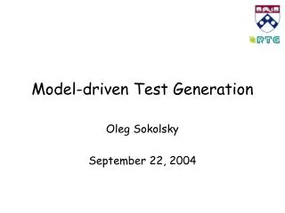
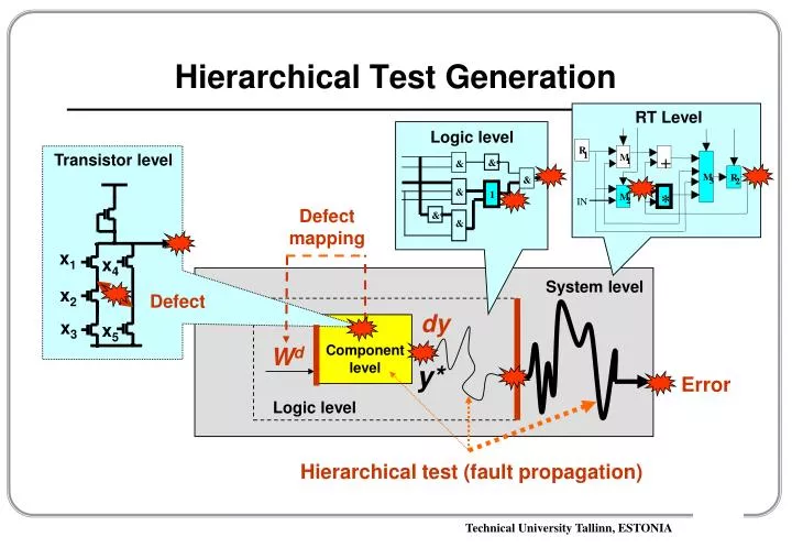
R. 1. M. +. 1. M. R. 3. 2. *. M. 2. IN. &. &. &. &. 1. &. &. Hierarchical Test Generation. RT Level. Logic level. Transistor level. Defect mapping. x 1. x 4. System level. x 2. Defect. dy. x 3. x 5. Component level. W d. y*. Error. Logic level.

E N D
R 1 M + 1 M R 3 2 * M 2 IN & & & & 1 & & Hierarchical Test Generation RT Level Logic level Transistor level Defect mapping x1 x4 System level x2 Defect dy x3 x5 Componentlevel Wd y* Error Logic level Hierarchical test (fault propagation)
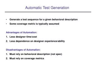
y 1 x1 1 0 x2 x3 x4 x5 x6 x7 0 Binary Decision Diagrams Functional BDD Simulation: 0 1 1 0 1 0 0 Boolean derivative:
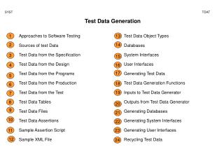
Generalization of BDDs Binary DD 2 terminal nodes and 2 edges from each node General case of DD n 2 terminal nodes and n 2 edges from each node y Gy 0 l1 1 l0 Y lm GY 1 l1 m 2 lm m l2 lh l0 h lk ln lk+1 Fk 0 Fn Fk+1 Novelty: Boolean methods can be generalized in a straightforward way to higher functional levels
Faults and High-Level Decision Diagrams K: (If T,C) RD F(RS1,RS2,…RSm), N RTL-statement: Terminal nodes RTL-statement faults: data storage, data transfer, data manipulation faults Nonterminal nodes RTL-statement faults: label, timing condition, logical condition, register decoding, operation decoding, control faults
Fault Modeling on DDs • Each path in a DD describes the behavior of the system in a specific mode of operation • The faults having effect on the behaviour can be associated with nodes along the path • A fault causes incorrect leaving the path activated by a test
Uniform Formal Fault Model on DDs D1:the output edge for x(m) = i of a node mis always activated D2:the output edge for x(m) = i of a node mis broken D3:instead of the given edge, another edgeor a set ofedges is activated
Fault Collapsing with SSBDDs Each node in SSBDD represents a signal path: Two SSBDD faults x111, x110 represent a set of six faults in the circuit: {x111, x61, y1; x110, x60, y0}
Structural HLDDs Each node in SSBDD represents a signal path: The faults at y3 in HLDD represent the faults in the control circuitry and in the multiplexer M3 of the RTL circuit The faults at R1*R2 in HLDD represent the faults in multiplier, input and output buses, and in the registers Fault collapsing – not investigated at high-level
I1: MVI A,D A IN I2: MOV R,A R A I3: MOV M,R OUT R I4: MOV M,A OUT IA I5: MOV R,M R IN I6: MOV A,M A IN I7: ADD R A A + R I8: ORA R A A R I9: ANA R A A R I10: CMA A,D A A Decision Diagrams for Microprocessors DD-model of the microprocessor: Instruction set: 1,6 A I IN 3 2,3,4,5 I R OUT IN 4 7 A + R A 8 2 A R I A R 9 A R 5 IN 10 A 1,3,4,6-10 R
Decision Diagrams for Microprocessors High-Level DD-based structureofthe microprocessor (example): DD-model of the microprocessor: 1,6 A I IN IN 3 R 2,3,4,5 I R OUT A 4 7 A + R I A OUT 8 2 A R I A R 9 A R 5 A IN 10 A 1,3,4,6-10 R
From MP Instruction Set to HLDDs R3 R2 R0 R3 R2 R1 R0 R1 B0 B2 B1 B OP A B A1 = 0 A1 = 3 R(A1) R(A2) 0 0 A2 A1 Instruction code: ADD A1 A2 OP=2. B=0. A1=3. A2=2 R3 = R3 + R2 PC = PC+1 R0 R3 1 1 M(A) R(A2) R(A1) R(A1) R(A1) R(A1)+ R(A2) R(A1)- R(A2) 2 2 3 3 M(A) 1 0 R(A2) OP 1-3 0 M(A) R0 1 0 0 PC 0 OP PC + 2 1 0 1, 2 PC + 1 1 0 3 0 1 R1, R2 1 0 2 0 R3 C 1 3 1 1 0
HLDDs for MP InstrSet R0 R1 R3 R2 R1 R2 R3 R0 B1 B2 B0 B OP A B A1 = 0 A1 = 3 R(A1) R(A2) 0 0 Instruction code: ADD A1 A2 OP=2. B=0. A1=3. A2=2 R3 = R3 + R2 PC = PC+1 A1 A2 R3 R0 1 1 Program Counter R(A1) R(A2) R(A1) R(A1) M(A) R(A1)+ R(A2) R(A1)- R(A2) 2 2 3 3 M(A) 1 0 R(A2) OP 1-3 0 M(A) Register Decoding Registers and ALU R0 1 0 0 1 0 PC 0 OP PC + 2 1 0 1, 2 1 PC + 1 R1, R2 Memory Access 3 0 0 2 R3 1 1 3 1 0 0 C 1
c (M) 1 Function y 1 = M R 0 1 1 = 1 M IN 1 d (M) 2 Function y 2 = 0 M R 2 1 = 1 M IN 2 e (M ) 3 Function y 3 = + 0 M M R 3 1 2 = 1 M I N 3 = 2 M R 3 1 = * 3 M M R 3 2 2 R 2 Operation Function y n 4 Reset = 0 0 R 2 Hold = ’ 1 R R 2 2 Load = 2 R M 2 3 Structural Synthesis of HLDDs Control Path y x Data Path
Data Path: High-Level DD Synthesis Control Path R 2 Operation Function y y 4 x Reset = 0 0 R 2 Hold = ’ 1 R R 2 2 Data Path Load = 2 R M 2 3 R 2 0 y # 0 4 1 R 2 2 e
Data Path: HLDD Synthesis R 2 0 y # 0 4 Control Path 1 R 2 y x 0 2 y c 3 Data Path R2 1 IN M 3 2 Function y R 3 1 = + 0 M M R 3 1 2 3 = 1 M I N 3 d = 2 M R 3 1 = * 3 M M R 3 2 2 R2 +e R 2 Operation Function y 4 Reset = 0 0 R 2 Hold = ’ 1 R R 2 2 Load = 2 R M 2 3
M 3 Function y 3 = + 0 M M R 3 1 2 = 1 M I N 3 = 2 M R 3 1 = * 3 M M R 3 2 2 R 2 Operation y 4 Data Path: HLDD Synthesis c (M) R 1 2 0 Function y y # 0 1 4 = M R 0 1 1 1 = 1 M IN R 1 2 c (M1) d (M) 2 0 0 2 Function y y y 2 R + R 3 1 1 2 = 0 M R R2 2 1 = 1 1 M IN 2 IN + R 2 1 IN 2 R 1 3 0 y R * R 2 R2 +M3 1 2 1 Function IN* R 2 Reset = 0 0 R 2 d (M2) Hold = ’ 1 R R 2 2 Load = 2 R M 2 3
R 2 0 y # 0 4 1 R 2 M1 0 0 2 y y R + R 3 1 1 2 R2 1 IN + R 2 1 IN 2 R 1 3 0 y R * R 2 R2 +M3 1 2 1 IN* R 2 M2 High-Level Decision Diagrams Superposition of High-Level DDs: A single DD for a subcircuit Instead of simulating all the components in the circuit, only a single path in the DD should be traced
BDDs for Flip-Flops – Functional Synthesis Elementary BDDs S D Flip-Flop J JK Flip-Flop q c D q D C S C K q’ c q’ R K R RS Flip-Flop q’ J q c S S R C q’ q’ U R R BDDs as a method for knowledge presentation U - unknown value
Functional Synthesis of High-Level DDs High-Level DDs can be synthesized by symbolic execution of the Data-Flow Diagram Data-Flow Diagram F2
Synthesis of High-Level DDs High-Level DDs can be synthesized by symbolic execution of the Data-Flow Diagram: Decision Diagrams: 1 AC 0 1 0 F0 AX F1 AC PC F2 AC F2 AC+1 AX AC=0 PC+1 0 1 AX PC
Data Path M Begin A s 0 ADR B A = B + C C s 1 z 1 0 1 MUX x 1 A z CC z A = A + 1 B = B + C 2 MUX 2 s s 4 2 1 0 0 1 y x x x A B CON D C = C B = B C = C s Control Path d l / 3 0 1 0 1 ¢ q x x q C C FF A = C + B A = A + B + C C = A + B s 5 END Digital System and Data Flow Diagram Data-Flow Diagram Digital system
Begin s 0 A = B + C s 1 1 0 x A A = A + 1 B = B + C s s 4 2 1 0 0 1 x x A B C = C B = B C = C s 3 0 1 0 1 x x C C A = C + B A = A + B + C C = A + B s 5 END Functional HLDDs Decision Diagrams Data Flow Diagram Register variables State variable
Synthesis of Functional HLDDs Results of cycle based symbolic simulation: Data Flow Diagram/FSMD q = 0 Begin q = 1 A = B + C 1 0 x A q = 2 q = 4 A = A + 1 B = B + C 1 0 0 1 x x A B q = 3 C = C B = B C = C 0 1 0 1 x x C C A = C + B A = A + B + C C = A + B q = 5 END
Synthesis of HLDDs Extraction of the behaviour for A: Results of symbolic simulation: Predicate equation for A: A =f (q, A, B, C, xA, xC) = = (q=0)(B+C) (q=1)(xA=0) (A + 1) (q=3)(xC=1)( C+B) (q=4)(xA=0)(xC=0)(A+ B + C + 1)
Synthesis of HLDDs Decision diagram for A: Extraction of the behaviour for A: Predicate equation for A: A = (q=0)(B+C) (q=1)(xA=0) (A + 1) (q=3)(xC=1)( C+B) (q=4)(xA=0)(xC=0)(A+ B + C + 1) Synthesis method: similar to Shannon’s expansion theorem:
Begin s 0 A = B + C s 1 1 0 x A A = A + 1 B = B + C s s 4 2 1 0 0 1 x x A B C = C B = B C = C s 3 0 1 0 1 x x C C A = C + B A = A + B + C C = A + B s 5 END Functional HLDDs Decision Diagrams Data Flow Diagram Register variables State variable
High-Level Vector Decision Diagrams A system of 4 DDs Vector DD 0 A 0 0 C ¢ B’ + C’ q M=A.B.C.q i ¢ q x A’ + B’ ¢ ¢ q B + C i A B q #1 1 0 #5 x ¢ A + 1 A 1 0 A 1 C x A’ + 1 i 3 1 A i C’ q x q ¢ ¢ C + B C #4 #3 4 0 0 1 B x x ¢ ¢ ¢ A + B + C C A B’ + C’ 0 0 A i q x x A’ + B’+C’ i A C 1 1 B #2 2 x ¢ ¢ ¢ B + C q B B’ A q 4 0 #5 3 0 C 0 x ¢ B A’ + B’ x ¢ q # A q 1 i B C q B’ i 2 0 1 0 #5 q x ¢ x # q ¢ ¢ 4 A + B C B A #5 1 A 1 B’ + C’ 1 3 i 0 1 C q x # 2 C’ i C #5 q 4 0 2 4 1 #5 x # 5 x B ¢ C A 1 3,4 # 3
DD Synthesis from VHDL Descriptions VHDL description of 4 processes which represent a simple control unit
DD Synthesis from VHDL Descriptions DDs forstate, enable_inand nstate 1 state rst #1 0 1 nstate clk 0 Superposition of DDs state’ 0 1 state’ nstate enable_in #1 1 2 0 #2 rb0 1 1 clk enable_in enable 0 enable’
state 1 rst #1 0 0 1 state’ #1 enable' 2 1 0 rb0 #2 1 0 1 outreg fin reg_cp reg enable state #0001 1 2 #0011 0 0 #1100 enable rb0 1 1 #0100 #0010 DD Synthesis from VHDL Descriptions DDs forthe total VHDL model
state 1 rst #1 0 0 1 state’ #1 enable' 2 1 0 rb0 #2 1 0 1 outreg fin reg_cp reg enable state #0001 1 2 #0011 0 0 #1100 enable rb0 1 1 #0100 #0010 DD Synthesis from VHDL Descriptions Simulation and Fault Backtracing on the DDs Simulated vector
Hierarchical Modelling on DDs System: High-level decision diagram 1 C A small part is simulated at the lower level x1 1 0 x3 x2 M=A.B.C.q 0 A 0 C ¢ B’ + C’ q i x5 x4 x A’ + B’ q i B q #1 #5 1 0 A 1 C x6 x7 x A’ + 1 i A i C’ q q #4 #3 Component: Binary Decision Diagram 1 B 0 B’ + C’ 0 0 A i q x x A’ + B’+C’ i A C B #2 2 B’ A small part is simulated at the higher level: to increase the speed of analysis q #5 3 0 C A’ + B’ x i B C Cause-effect analysis well formalized q B’ i #5 q #5 1 A B’ + C’ i 1 C q C’ i #5 q 4 #5