Download
1 / 16
160 likes | 436 Vues
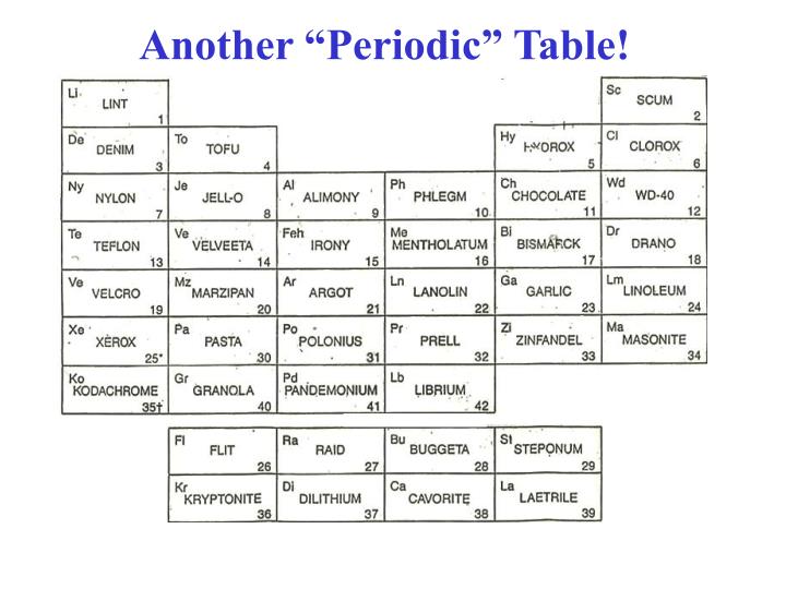
Another “Periodic” Table!. Growth Techniques Ch. 1, Sect. 2, YC. Czochralski Method (LEC) (Bulk Crystals) Dash Technique Bridgeman Method Chemical Vapor Deposition (CVD) (Thin films; epitaxial film growth) Metal-Organic Chemical Vapor Deposition (MOCVD)

E N D
Growth TechniquesCh. 1, Sect. 2, YC • Czochralski Method(LEC) (Bulk Crystals) • Dash Technique • Bridgeman Method • Chemical Vapor Deposition(CVD) (Thin films; epitaxial film growth) • Metal-Organic Chemical Vapor Deposition (MOCVD) • Molecular Beam Epitaxy(MBE) (Thin films) • Liquid Phase Epitaxy(LPE) (Thin films)
Czochralski Method Bridgeman Method a temperature gradient along the crucible growth speed ~ 2 - 3 mm/minute O, C are contaminants!
Thin Film Growth (General) • High Quality Film(1μm or less thickness) deposited on a high quality substrate. • To ensure high crystalline quality, the lattice parameters of the thin layer should match with that of the substrate(to minimize strain). Chemical Vapor Deposition (CVD) • Used for growing thin layers of perfect crystals. To ensure high crystalline quality, the lattice parameters of the thin layer should match with that of the substrate (to minimize strain). • Terminology(epitaxial growth): Homoepitaxy:When the thin crystal layer lattice is the same as that of the substrate (e.g. Si film on Si substrate). Heteroepitaxy:When the thin crystal layer lattice is different from that of the substrate (e.g.. GaAs film on Si).
Thin Film Growth Oh, its your standard “boy meets girl, boy loses girl, boy invents a new deposition technique for ultra-thin film semiconductors, boy gets girl back” story.
Chemical Vapor Deposition(CVD) • Epitaxial films can be grown from solid, liquid, or gas phases. It is easier to control the growth rate in gas phase epitaxy by controlling the flow of gases. • In CVD, gases containing the required chemical elements are made to react in the vicinity of the substrate inside the reactor. • Example reaction. (The temperature of the substrate plays an important role). SiH4 (heat) Si + 2 H2 (Silane gas) (on the substrate) (H2 gas) • The reaction occurs in a sealed container (reactor) NOTE!! Silane gas is highly toxic & highly explosive!! NOTE!! Hydrogen gas is highly explosive!!!!
Metal-Organic Chemical Vapor Deposition(MOCVD) • Example reaction: Ga(CH3)3 + AsH3 (Trimethal gallium gas) (Arsene gas) 3CH4 + GaAs (Methane gas) (on the substrate) • The reaction occurs in a sealed container (reactor) • NOTE!!Arsene gas is highly toxic & highly flammable! Trimethal gallium gas is highly toxic!! Methane gas is highly explosive! If you are British, MOCVD OMCVD!
MOCVD Dopants are introduced in precisely controlled amounts!
Molecular Beam Epitaxy(MBE) • Thin film growth under ultra high vacuum(~10-10 torr) • Reactants introduced by molecular beams. • Create beams by heating source of material in an effusion (or Knudsen) cell. • Several sources, several beams of different materials aimed at substrate Can deposit 1 atomic layer or less! • A very precisely defined mixture of atoms to give EXACTLY the desired material composition!
MBE Source molecular beam comes out here Source is in here r r
MBE Setup complex & expensive!
RHEED: Used with MOCVD & MBE electron beam probe to monitor surface film quality One period of oscillation growth of one atomic layer of GaAs (or whatever material)
MOCVD vs. MBE MBE Mainly useful for research lab experiments. Not efficient for mass production! MOCVD Useful for lab experiments & for mass production! MANY MILLIONS OF $$$$ FOR BOTH!!!!!
MOCVD vs. MBE Molecular Beam Expitaxy (MBE) Metal-Organic Chemical Vapor Deposition (MOCVD) • Both of these techniques allow crystals to be deposited on a substrate one monolayer at a time with great precision. • These techniques are very useful for artificial crystal structures such as “superlattices” and “quantum wells”. Differences between MBE and MOCVD MOCVD Gases are let into the reactor at high pressure ~ 1 torr MBE Always done under UHV conditions, with pressures below 10-8 torr
Liquid Phase Epitaxy (LPE)(GaAs & other III-V materials) • A group III metal utilized as a solvent for As • The solvent is cooled in contact with (GaAs) substrate. Becomes saturated with As. Nucleation of GaAs on the substrate. • A slider, containing different solutes, can grow precise compositions of material.