Download
1 / 61
650 likes | 778 Vues
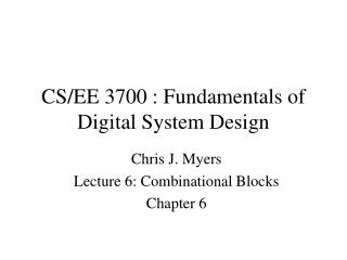
CS/EE 6710. CMOS Processing. N-type Transistor. D. G. S. +. Vds. i. electrons. -. +Vgs. N-type from the top. Top view shows patterns that make up the transistor. Diffusion Mask. Mask for just the diffused regions. Polysilicon Mask. Mask for just the polysilicon areas.

E N D
CS/EE 6710 CMOS Processing
N-type Transistor D G S + Vds i electrons - +Vgs
N-type from the top • Top view shows patterns that make up the transistor
Diffusion Mask • Mask for just the diffused regions
Polysilicon Mask • Mask for just the polysilicon areas
Combine the two masks • You get an N-type transistor • There are other steps in the process…
A Cutaway View • CMOS structure with both transistor types
Look at Inverter Layout Again • How many layers? • How many processing steps?
Photolithography UV Light • Oxidation Layer • Photoresist (PR) Coating • Stepper Exposure • PR development and bake • Acid Etching • Spin, Rinse, Dry • Processing step • PR removal (ashing)
Growing the Silicon Crystal • Need single crystal structure • Single crystal vs. Polycrystalline silicon (Poly)
Czochralski Method • Need single-crystal silicon to accept impurities correctly • Donor elements provide electrons • Acceptor elements provide holes • Pull a single crystal of silicon from a puddle of molten polycrystalline silicon
Slice Crystal into Wafers • Slice into thin wafers (.25mm - 1.0mm), and polish to remove all scratches
Oxidation, Growing SiO2 • Essential property of silicon is a nice, easily grown, insulating layer of SiO2 • Use for insulating gates (“thin oxide”) • Also for “field oxide” to isolate devices
Adding Photoresist • Photoresist can be positive or negative • Does the exposed part turn hard, or the unexposed part?
“Steppers” Expose the Mask • Use very short wavelength UV light • Single frequency, 436 - 248 nm • Expensive! ~$5,000,000/machine…
Develop and Bake Photoresist • Developed photoresist is soft, unexposed is hardened • So you can etch away the soft (exposed) part
Now Etch the SiO2 • Etch the SiO2 to expose the wafer for processing • Then Spin Rinse, and Dry
Add a Processing Step • Now that we’ve got a pattern etched to the right level, we can process the silicon • Could be: • Ion Implantation (I.e. diffusion) • Chemical Vapor Deposition (silicide, Poly, insulating layers, etc.) • Metal deposition (evaporation or sputtering) • Copper deposition (very tricky)
Ion Implantation • Implant ions into the silicon • Donor or Acceptor
Metal Deposition • Typically aluminum, gold, tungsten, or alloys
Copper is Tricky • 40% less resistance than Aluminum • 15% system speed increase • But, copper diffuses into Silicon and changes the electrical properties
Final Layer: Passivation • Basically a final insulating layer (SiO2 or Si3N4) to protect the circuit
CMOS Fabrication • Start from single-crystal silicon wafer • Use photolithography to pattern device layers • Essentially one mask/photolithographic sequence per layer • Built (roughly) from the bottom up • 6 - Metal 3 • 5 - Metal 2 • 4 - Metal 1 • 2 - Polysilicon • 3 - Diffusions • 1 Tub (N-well) Via Via Contact Exception
Self-Aligned Gates • Thinox in active regions, thick elsewhere • Deposit Polysilicon • Etch thinox from active region (Poly serves as mask for etch/diffusion) • Implant dopant
Another View of Fab • Taken from slides by Jan Rabaey • From his text “Digital Integrated Circuits”
Circuit Under Design This two-inverter circuit (of Figure 3.25 in Rabaey’s text ) will be manufactured in a twin-well process.
Start Material Starting wafer: n-type with doping level = 10 13 3 /cm A A’ * Cross-sections will be shown along vertical line A-A’
N-well Construction (1) Oxidize wafer (2) Deposit silicon nitride (3) Deposit photoresist