Download
1 / 23
240 likes | 370 Vues
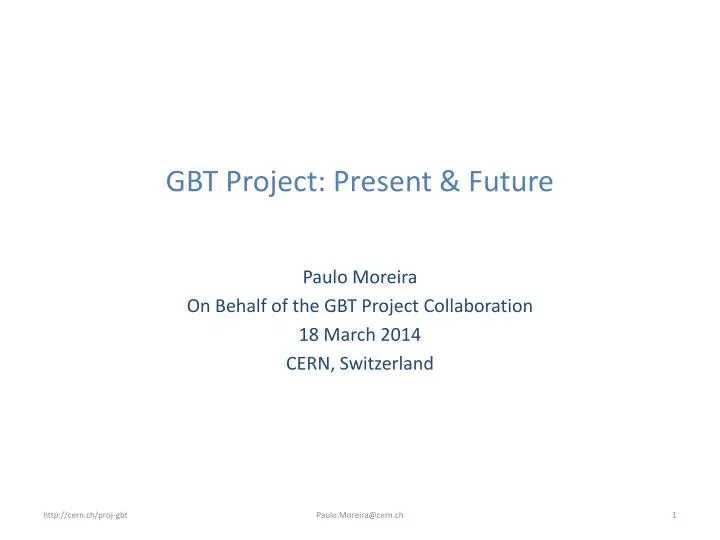
GBT Project: Present & Future. Paulo Moreira On Behalf of the GBT P roject Collaboration 18 March 2014 CERN, Switzerland. Outline. Radiation Hard Optical Link Architecture The GBT System GBT Chipset: Status Schedule GBT-FPGA Status GBT Building Blocks Status LpGBTX: Architecture

E N D
GBT Project: Present & Future Paulo Moreira On Behalf of the GBT Project Collaboration 18 March 2014 CERN, Switzerland Paulo.Moreira@cern.ch
Outline • Radiation Hard Optical Link Architecture • The GBT System • GBT Chipset: • Status • Schedule • GBT-FPGA Status • GBT Building Blocks Status • LpGBTX: • Architecture • SerDes (Resources optimization) • Power Consumption • Footprint • Project effort Paulo.Moreira@cern.ch
Radiation Hard Optical Link Architecture GBT GBT Versatile Link FPGA Timing & Trigger Timing & Trigger GBTX PD GBTIA DAQ DAQ LD GBLD Slow Control Slow Control Custom ASICs On-Detector Radiation Hard Electronics Off-Detector Commercial Off-The-Shelf (COTS) Paulo.Moreira@cern.ch
The GBT System External clock reference FEModule Clock[7:0] E – Port e-Link GBTX Phase - Shifter CLK Reference/xPLL E – Port FEModule E – Port ePLLRx GBTIA DEC/DSCR CDR E – Port data-down data-up Phase – Aligners + Ser/Des for E – Ports CLK Manager clock 80, 160 and 320 Mb/s ports GBLD SCR/ENC SER E – Port ePLLTx FEModule E – Port E – Port One 80 Mb/s port Control Logic Configuration (e-Fuses + reg-Bank) GBT – SCA JTAG I2C Slave I2C Master E – Port I2C (light) data JTAG Port I2C Port control clocks Paulo.Moreira@cern.ch
GBLD Status GBLD V4.1 • Main Specs • Bit rate 5 Gb/s (min) • Modulation: • Current sink • Single-ended/differential • Laser modulation current: 2 to 24 mA • Laser bias: 2 to 43 mA • Equalization: • Pre-emphasis/de-emphasis • Independently programmable for rising/falling edges • Supply voltage: 2.5 V • Die size: 2 mm × 2 mm • I2C programming interface • Status • Available in small quantities • Integrated in the VTRx and VTTx • Fully functional • Excellent performance • Radiation hardness proved (total dose) • Heavy Ion and Neutron SEU tests: • Revealed “some sensitivity” of the configuration registers • Proton tests shown no upsets • Majority of the errors related with reset function (not triplicated) can be easily improved. • Technology: 130 nm DM metal stack • Device is production ready 4.8 Gb/s, pre-emphasis on Total jitter: ≈ 25 ps Paulo.Moreira@cern.ch
GBTIA Status GBTIA V2.0 / V2.1 • Main specs: • Bit rate 5 Gb/s (min) • Sensitivity: 20 μA P-P (10-12 BER) • Total jitter: < 40 ps P-P • Input overload: 1.6 mA (max) • Dark current: 0 to 1 mA • Supply voltage: 2.5 V • Power consumption: 250 mW • Die size: 0.75 mm × 1.25 mm • Status: • Fully functional • Integrated in the VTRx • Excellent performance • Radiation hardness proved • Tested up to 200 Mrad (SiO2) • Device is production ready • LM metal stack Paulo.Moreira@cern.ch
GBTX Status • Main specs: • 4.8 Gb/s transceiver • User bandwidth: • 3.28 Gb/s up/down-links, GBT mode • 3.52 Gb/s up-link, 8B/10B mode • 4.48 Gb/s up-link, wide-bus mode • Status: • Chip is fully functional • A few modifications will be introduced in the production version: • XPLL will be adapted for a higher value of the motional resistance of the quartz crystal • Tolerance to SEUs of the e-link programing register will be improved • Startup state machine expanded • Prototypes availability: • 22 + 32 (drilled) GBTX available • Additional 240 will be available in August Total height including solder balls: ~3 mm 17 mm Paulo.Moreira@cern.ch 17 mm
GBT – SCA GBT Slow Control Adapter: • ASIC dedicated to slow control functions. • System Upgrades for SLHC detectors. • “Replacement” for the CCU & DCU ASICs • Flexible enough to match the needs of different Front-End systems. Key Features: • Dual redundant e-Ports for GBTX e-links. • 16 I2C master controllers @ 100k/s or1 Mb/s. • 1 SPI master controller • 1 JTAG master controller • 32 multiplexed ADC channels: • 12-bit dual slope integrating ADC @ 3.5KHz • 4 DAC channels • 32 Digital I/O lines individually programmable. • 8-bit memory bus • 4 Interrupt inputs • Technology: CMOS 130nm using radiation tolerant techniques. Status: • Chip ready for prototyping: • Tapout May 2014 Total height including solder balls: ~3 mm 11.6 mm Paulo.Moreira@cern.ch 11.6 mm
GBT Chipset Schedule “Scenario 1” – MPW followed by production • 19 May2014 – MOSIS MPW • GBTX • GBT - SCA • GBLD • Q3 – 2014 • Chips available from the foundry • ASIC Packaging • Q4 – 2014 • Prototypes medium quantities: ~200 • Samples distributed to the users • Q1 – 2015: • Launch the production • Q3 – 2015: • Production quantities available “Scenario 2” – Production only • Q2 – 2014 (May) • Split Engineering Run to produce in quantities: • GBTX • GBTIA • GBLD V4 • GBT - SCA • Q3 – 2014 • Chips available from the foundry • ASIC Packaging • Q4 – 2014 • ASIC production testing • First production ASICs distributed to the users Paulo.Moreira@cern.ch
GBT – FPGA Status • Aim: • Implement the GBT serial link in all its flavours as an IP core for most of the current FPGAs used on Back-End boards for upgrades • Firmware versions • Serial link encoding schemes • Reed-Solomon (aka “GBT frame” ), • 8b/10b (to be done) • Wide-bus • Standard and Fixed latency versions • Targeted FPGA and reference design • Altera: • Cyclone V GT • Eval kit & GBTx-SAT board • Stratix V • AMC 40 • Xilinx: • Virtex 6 • ML605 & GLIB • Kintex 7 • KC705 • Virtex 7 • VC705 • Project Resources • 50% of one Fellow since last summer • More than 85 users registered • A sharepoint site: https://espace.cern.ch/GBT-Project/GBT-FPGA/default.aspx • A SVN repository: • https://svnweb.cern.ch/cern/wsvn/ph-ese/be/gbt_fpga • Contact us: • Sophie.Baron@cern.ch • Manoel.Barros.Marin@cern.ch MAJOR RELEASE 11 APRIL 2014 See poster by Manoel Barros forfurther information on the GBT – FPGA Paulo.Moreira@cern.ch
GBT Building Blocks (IP) Status Available “IP” to facilitate the implementation ofe-Link transceivers in the frontend ASICs: • SLVS Receiver • Wire-bond, DM metal stack • C4, LM metal stack • SLVS Driver • Wire-bond, DM metal stack • C4, LM metal stack • SLVS Bi-directional • C4, LM metal stack • HDLC transceiver • Synthesizable Verilog • 7B/8B CODEC • Synthesizable Verilog • ePLL-FM • Frequency MultiplierPLL • Radiation Hard • 130 nm CMOS technology with the DM metal stack (3-2-3). • Input frequencies: 40/80/160 MHz • Output frequencies: 160/320 MHz regardless the input frequency • Programmable phase of the output clocks with a resolution of 11.25° for the 160 MHz clock and 22.5° for the 320 MHz clock • Programmable charge pump current, loop filter resistance and capacitance to optimize the loop dynamics • Supply voltage: 1.2 V - 1.5 V • Nominal power consumption: 20 mW @ 1.2 V - 30 mW @1.5 V • Operating temperature range: -30°C to 100°C • ePLL-CDR (currently under testing) • Data rate: 40/80/160/320 Mbit/s • Output clocks: data clock + 40/80/160/320 MHz with programmable phase • Internal or external calibration of the VCO frequency • Possibility to use it as a frequency multiplier PLL without applying input data • Programmable charge pump current, loop filter resistance and capacitance to optimize the loop dynamics • Supply voltage: 1.2 V - 1.5 V • Operating temperature range: -30°C to 100°C • Prototype fabrication: May 2013 ePLL- FM Paulo.Moreira@cern.ch
The LpGBTX • Low Power Dissipation and Small Footprint: • Critical for pixel detectors • Critical for tracker/triggering detectors • Bandwidth: • Low-Power mode • 4.8 Gb/s for Up and Down links • High-Speed mode: • 9.8 Gb/s for the Up-link • 4.8 Gb/s for the Down-link • e-Links: • 80, 160 and 320 Mb/s for down-links • Low-Power Mode: • 80, 160 and 320 Mb/s for up-links • High-Speed Mode: • 160, 320 and 640 Mb/s for up-links • Programmable: Single-ended / differential • Functionality: • “Replica” of the GBTX • Small subset of the GBT-SAC functionality will be included Paulo.Moreira@cern.ch
LpGBTXArchitecture “Idle & data headers” could be used to distinguish between the “odd and even frames”when operating at 9.6 Gb/s! SerDes DEC & DSCR ePortTx eLinkOut[39:0] rxData[79:0] 4.8 Gb/s ecOut cdrOut[119:0] rxEcData[1:0] eClock39:0] refClk40MHz 160/320 MHz 40/80/160/320/640 MHz 40 MHz 160/320/640 MHz 40 MHz 160/320/640 MHz eLinkIn[39:0] ePortRx SCR & ENC txData[159:0] eLinkIn[57:40] txData[223:160] serIn[239:0] 4.8 or 9.6 Gb/s ecIn[1] txEcData[3:0] SCA (Reduced set) PhaseShifter • Downlink: 4.8 Gb/s • GBT mode • Uplink: 4.8/9.6 Gb/s • GBT / Wide-Bus / 8B/10B • EC link: 80 Mb/s • SCA functionality added • Output e-Links: • 80/160/320 Mb/s 40 e-Links (max) • Phase programmable clocks: • 40/80/160/320/640 MHz 8 Clocks (max) • Output e-Clocks: • 40/80/160/320 Mb/s 40 e-Clocks (max) • Input-Links: • 80/160/320 Mb/s @ 4.8 Gb/s • 160/320/640 Mb/s @ 9.6 Gb/s • GBT mode 40 e-Links (max) • Wide-bus mode 56 e-Links (max) Newcomer! Paulo.Moreira@cern.ch
SerDes Optimization • 1 high frequency PLL drives the CDR and SER: • Half Rate CDR (same architecture as GBTX) • Serializer: • Full rate @ 4.8 Gb/s • Half rate @ 9.6 Gb/s • PLL can work as: • CDR • Frequency Multiplier • This enables: TX, RX and TRANS Clock Divider • For the e-Links the clock frequencies are: • 40/80/160/320/640 MHz • Half rate CDR requires: • 2.4 GHz • I and Q phases • Differential for CML • Serializer: Half rate 9.8 Gbps / Full rate 4.8 Gbps • 4.8 GHz For efficiency the SER and DES have to be co-designed De-Serializer cdrOut[119:0] 4.8 Gb/s CDR/FM PLL 1/N refClk40MHz 40/80/160/320/640 MHz Oscillator Serializer Aided Lock Control 4.8 or 9.6 Gb/s serIn[239:0] Paulo.Moreira@cern.ch
LpGBTX: Power (1/2) LpGBTX power estimate • Assumes: • 65 nm CMOS technology • Supply voltage: 1.2V • Merged SerDes architecture • 4.8 Gb/s on both up and down links • e-Links with 200 mV signaling • “SCA” functionality not taken into account in this preliminary study Preliminary & Non-Binding! Paulo.Moreira@cern.ch
LpGBTX: Power (2/2) Case study: • Hypothetical configuration: • E-Links: • 20 × Data-In @ 160 Mb/s • 1 × Clock @ 160 MHz • 2 × Data-Out @ 160 Mb/s • Phase-Adjustable clocks: • 2 × Clock @ 40 MHz • 2 × Clock @ 160 MHz Preliminary & Non-Binding! Paulo.Moreira@cern.ch
LpGBTX: Footprint General Purpose LpGBTX with programmable I/O (Single-ended /Differential) Tracker Specific Development (Single-ended I/O only) • Two ASICs: • LpGBT-SerDes (tracker specific)! • LpGBTX (general purpose) • Although many functions are the same in the • two ASICs, these are effectively two projects! • Almost doubles the budget and the manpower needs! I/O set to single-ended I/O set to differential Preliminary & Non-Binding! • Pin-count: ≈ 150 (to be confirmed) • BGA pitch: 0.65 mm • Package Size: ≈ 10 mm × 10 mm • Pin-count: ≈ 500 • BGA pitch: 0.65 mm • Package Size: ≈ 16 mm × 16 mm Paulo.Moreira@cern.ch
LpGBTX: 2014 – and beyond, Activities / Manpower / Budget 2014 • Q3: First draft of LpGBTX specifications • Q3: Discussions with the Experiments • Q4: LpGBTX final specifications 2015 and beyond • LpGBTIA • (The GBTIA is already relatively low power. Perhaps the LpGBTIA is not a strictly necessary development…) • Technology: 65 nm CMOS • Manpower: 2 MY (design and testing) • LpGBLD10 • (Some work already going on) • Technology: 130 nm CMOS • Manpower: 2 MY (design , packagingand testing) • LpGBTX • Technology: 65 nm CMOS • Two packaging flavours: • “Tracker” & “General Purpose” • Manpower: • Design: 8 MY • Packaging: 1 MY • Testing: 2 MY • We have to seriously consider “building” a stable LpGBT team if a LpGBT chipset is to be a reality in useful time! • The move to 65 nm and Low Power is not just a “copy-paste exercise”!!! • The LpGBT has not yet been defined as an approved “project” or “common project”: • Effort going on to secure budget and manpower for the project! Total manpower: 15 MY Paulo.Moreira@cern.ch
Extra Slides Paulo.Moreira@cern.ch
DOWNLINK BACK END FRONT END CLOCK GBTx SAT board GLIB Cyclone V GBT-FPGA GBTx FE EMULATOR PLL GBT SERDES CDR E-LINK SERDES GBT-FPGA TX MGT TX E-LINK SERDES SFP SFP GBT-FPGA RX MGT RX CDR EportRx: phase-aligner (set to maximum and minimum; FE position dependant) EportTx: no phase alignnecessary on GBTx Flags are latchedwith e-link’sclock and triggered by the e-links data GBT-FPGA uplink and downlink flag latched with 40 MHz clock UPLINK M. Barros Marin, P. Leitao, S. Baron
DOWNLINK BACK END FRONT END CLOCK 29 ns 21 ns GBTx SAT board GLIB Cyclone V GBT-FPGA GBTx FE EMULATOR PLL GBT SERDES CDR E-LINK SERDES GBT-FPGA TX MGT TX E-LINK SERDES SFP SFP GBT-FPGA RX MGT RX CDR 1 ns 5 ns 4 ns 51.2 ns 30.6 ns UPLINK M. Barros Marin, P. Leitao, S. Baron
UPSTREAM LATENCY Remaining: MGT, SFPs, GBTx M. Barros Marin, P. Leitao, S. Baron
DOWNSTREAM LATENCY Remaining: MGT, SFPs, GBTx M. Barros Marin, P. Leitao, S. Baron