Download
1 / 1
10 likes | 131 Vues
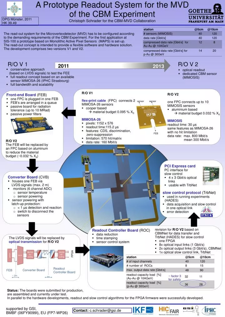
A Prototype R eadout S ystem for the MVD of the CBM Experiment Christoph Schrader for the CBM-MVD Collaboration. DPG Münster, 2011 HK 39.49. 1Gbit/s fibers. 8b/10b en- coding. 10b/8b de- coding. . . . . . . . . . FPGA. . . . MUX. sensor.

E N D
A Prototype Readout System for the MVD of the CBM Experiment Christoph Schrader forthe CBM-MVD Collaboration DPG Münster, 2011 HK 39.49 1Gbit/s fibers 8b/10b en- coding 10b/8b de- coding . . . . . . . . . FPGA . . . MUX sensor The read-out system for the Microvertexdetector(MVD) has to be configured according to the demanding requirements of the CBM Experiment. For the first application at SIS-100 a prototype based on Monolithic Active Pixel Sensors (MAPS) is set-up. The read-out concept is intended to provide a flexible software and hardware solution. The development comprises two versions V1 and V2. Readout Controller Board Converter Board FEB ~ 2m >> R/O V 1 R/O V 2 2011 2013 • conservative approach • (based on LVDS signals) to test the FEE • full readout concept based on an available sensor MIMOSA-26 (IPHC Strasbourg) • full bandwidth and scalability • optical readout • dedicated CBM sensor (MIMOSIS) R/O V2 • one FPC connects up to 10 MIMOSIS sensors • aluminium based • material budget 0.032 % X0 MIMOSIS readout time: 30 µs same features as MIMOSA-26 with no hit limitation data rate: max. 800 Mbit/s • mean 300 Mbit/s • R/O V1 • flex-print cable(FPC) connects 2 MIMOSA-26 sensors • cooper based • material budget 0.095 % X0 MIMOSA-26 • pixels: 1152 x 576 • readout time:115.2 µs • features: CDS, discrimination, • zero-suppression • limitation: 570 hit/matrix • data rate: 160 Mbit/s sensor sensor FEB R/O V2 The FEB will be replaced by an FPC based on aluminum to reduce the material budget (~0.032 % X0) • Front-end Board (FEB) • one FPC is plugged in one FEB • FEB’s are arranged in a queue • passive board for radiation tolerance (up to 10 MRad) • passive power filters • Converter Board (CVB) • houses one FEB via • LVDS signals (max. 2 m) • monitors (6 channel ADC) • sensor temperature • sensor powering • sensor powering with • latch-up protection: • < 1 µs detection and reaction • switch to disconnect the • sensors • PCI Express card • PC interface for • slow control • 4 x 3 Gbit/s optical • links • usable with TrbNet • slow control protocol (TrbNet) • used in running experiments • (HADES) • data acquisition and slow control • in one optical link • error detection • revision for R/O V2 based on • CBMNet for data transfer and • TrbNet(HADES) for slow control • one FPGA • 8x optical input links (1 Gbit/s) • 2x optical output links (3 Gbit/s), CBMNet • 1x optical slow control link, TrbNet • Readout Controller Board (ROC) • data reduction • time stamping • sensor control system The LVDS signals will be replaced by optical transmissionfor R/O V2 ~ factor 3 for safety Status:The boards were submitted for production, are assembled and currently under test. In parallel to the hardware developments, readout and slow control algorithms for the FPGA firmware were successfully developed. Contact: c.schrader@gsi.de