Download
1 / 54
540 likes | 560 Vues
Explore the Spartan architecture for FPGA design, covering top-level attributes, CLB slices, I/O blocks, clock management, power modes, and memory options like RAM and shift registers. Dive into VHDL synthesis, CLB design, and clock distribution for optimal hardware implementation.

E N D
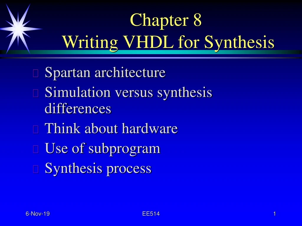
Spartan architecture Simulation versus synthesis differences Think about hardware Use of subprogram Synthesis process Chapter 8 Writing VHDL for Synthesis EE514
Spartan Architecture • Features • Top-level architecture and attributes • Configurable logic block (CLB) • Memory • I/O block • Three-state buses • Clocks and delay-locked loops • Power down mode • Configuration
Spartan Top-level Architecture • Configurable logic blocks • Implement logic here! • I/O blocks • Communicate with other chips • Choose from 16 signal standards • Block RAM • On-chip memory for higher performance EE514
Spartan Top-level Architecture • Clocks and delay locked loops • Synchronize to clock on and off chip • Rich interconnect resources • Three-state internal buses • Power down mode • Lower quiescent power EE514
CLB Slice (Simplified) • 1 CLB holds 2 slices which • have two sets of the following: • Four-input LUT • Any 4-input logic function • Or 16-bit x 1 RAM • Or 16-bit shift register • Carry & control • Fast arithmetic logic • Multiplexer logic • Storage element • Latch or flip-flop • Set and reset • True or inverted inputs • Sync. or async. control EE514
CLB Slice MUXF6 MUXF5 Slice MUXF5 LUT LUT LUT LUT Dedicated Expansion Multiplexers • MUXF5 combines 2 LUTs to form • 4x1 multiplexer • Or any 5-input function • MUXF6 combines 2 slices to form • 8x1 multiplexer • Or any 6-input function EE514
Dedicated 16x16 Multiplier Logic • Highly efficient ‘shift & add’ implementation EE514
LUT Q Q Q Q IN D D D D CE CE CE CE CE CLK OUT CLB Slice Slice LUT LUT LUT LUT ADDR[3:0] Look-up Table Shift Registers • Each LUT can be configured as shift register • Serial in, serial out • Dynamically addressable delay up to 16 cycles 0 1 2 15 EE514
LUT Q Q Q Q IN D D D D CE CE CE CE CE CLK OUT CLB Slice Slice LUT LUT LUT LUT ADDR[3:0] Flexible Cycle Delays • Use for programmable clock delay • Cascade for greater cycle delays • Use CLB flip-flops to add depth EE514
SDRAM ZBTRAM SSRAM SGRAM DSP Coefficients Small FIFOs Shallow/Wide 16x1 Distributed RAM External RAM megabytes bytes Memory Bandwidth and Flexibility • Spartan on-chip SelectRAM+TM memory Large FIFOs Packet Buffers Video Line Buffers Cache Tag Memory Deep/Wide 4Kx1 2Kx2 1Kx4 512x8 256x16 Block RAM kilobytes 200 MHz Memory Continuum Highest performance FPGA memory system EE514
W R Port A Spartan-II Dual-R/WPort Block RAM Port B R W W W R R Block RAM Provides 4K Bits Each • Dual read/write ports, each with: • Independent clock, R/W, and enable • Independently configurable data width from 4Kx1 to 256x16 Data Flow Spartan-II A to B Yes B to A Yes A to A Yes B to B Yes EE514
Block RAM Timing • Clock-to-output (glitch-free): 2.5 ns typ. • Address/data input setup: 1.0 ns typ. • Lookup table based RAM provides additional small memories (16x1) • Same timing as CLB logic • Both easily initialized at configuration to simulate ROM EE514
I/O Block (Simplified) • Registered input, output, 3-state control
IOBs Organized As Independent Banks • Up to eight banks on a device • Each bank can support any of the 16 signal standards • Logic level translation • Boards with mixed standards
SSTL HSTL SDRAM LVTTL LVCMOS CTT SRAM GTL+ Spartan-II As Center forSignal Translation • Chip to Chip • LVTTL, LVCMOS • Chip to Memory • SSTL2-I, SSTL2-II, SSTL3-I, • SSTL3-II, HSTL-I, HSTL-III, • HSTL-IV, CTT • Chip to Backplane • PCI33-5V, PCI33-3.3V, • GTL, GTL+, AGP EE514
Vector Based Interconnect 2ns 2ns 2ns 2ns CLB Array High Performance Routing • Hierarchical routing • Sparse longer connections for high speed • Routing delay depends primarily on distance • Predictable for early design analysis EE514
General Clock Support • Four dedicated global low skew buffers • Dedicated input pin (clock distribution only) • PCI with 500-ps maximum skew • Additional shared resources (e.g., long lines) • Distribute low-skew/high-fanout signals • Four delay-locked loops on each device • Two global buffers with each DLL pair EE514
Delay-locked Loop Functions • Eliminate clock distribution delay • System synchronization • Phase-shifted clocks • Clock multiplication and division • Clean up clocks with 50/50 duty cycle correction • Clock lock for synchronization • DLL feedback connected internally or externally • Can synchronize to DLL lock EE514
Improved Clock-to-out Using DLL • Clock-to-out delays reduced over 50% Output standard = LVTTL Fast 16mA Temp=room, Vdd=2.5V, Vcco=3.3V Waveforms: 1: CLKIN 2: DATA OUT (no DLL) 3: DATA OUT (DLL deskewed) Timing w/o DLL w/ DLL r->r r->f r->r r->f 3.6n 3.5n 1.4n 1.4n EE514
Spartan-II DLLs ImproveClock Networks Deskew Clocks on Board DLL1 DLL2 Deskew Clocks on Chip Cascade DLLs Manage up to 4 System Clocks Convert Clock Levels using Select I/O DLL3 DLL4 • Generate • Clocks • multiply • divide • shift Delay locked loops synchronize on-chip and board level clocks EE514
Power-down Mode • Controlled by single power down pin • All inputs blocked, appear low internally • All outputs disabled • All register states preserved • Power-down status pin • Synchronous wake up • 100 uA typical EE514
Configuration Modes There are four ways to program a Spartan FPGA EE514
Partial Reconfiguration • Frame by frame reconfiguration supported while device is running • Routing changes affect device operation • Re-initializing a block RAM requires stopping all access in that column • Can dynamically load the required logic at any time • Minimizes cost by time-multiplexing the logic resources EE514
MIPS • >200 MicroBlaze Processors fit in Virtex V5 • Effective cost per MicroBlazeprocessor $1.4 EE514
Simulation versus synthesis differences The process sensitivity list has a major impact on the preceding simulation of the corresponding process statement. The synthesis tools usually ignore the process sensitivity list and are able to generate corresponding hardware. latch : process (LATCH_EN, AD) begin if (LATCH_EN = '1') then ADDR_LATCH <= AD; end if; end process; EE514
Think about hardware architecture RTL2 of LE64 is begin process (data1, data2) variable x, y, z : unsigned (64 downto 0); begin x := '0' & unsigned(DATA1); y := '0' & unsigned(DATA2); z := y - x; if (z(64) = '0') then LE <= '1'; else LE <= '0'; end if; end process; end RTL2; library IEEE; use IEEE.std_logic_1164.all; use IEEE.std_logic_arith.all; entity LE64 is port ( DATA1 : in std_logic_vector(63 downto 0); DATA2 : in std_logic_vector(63 downto 0); LE : out std_logic); end LE64; architecture RTL1 of LE64 is begin LE <= '1' when (data1 <= data2) else '0'; end RTL1; EE514
Think about hardware Both architectures build the same function, however the second one will synthesize with less hardware since no comparator is inferred RTL1 has delay 31 ns (FPGA synthesized 298 ns) RTL2 has delay 15 ns (FPGA synthesized 124 ns) architecture RTL1 of LE64 is begin LE <= '1' when (data1 <= data2) else '0'; end RTL1; EE514
Think about hardware EE514
Think about hardware architecture RTL2 of LE64 is begin process (data1, data2) variable x, y, z : unsigned (64 downto 0); begin x := '0' & unsigned(DATA1); y := '0' & unsigned(DATA2); z := y - x; if (z(64) = '0') then LE <= '1'; else LE <= '0'; end if; end process; end RTL2; EE514
Think about hardware EE514
Think about hardware Use concurrent signal assignments if possible library IEEE; use IEEE.std_logic_1164.all; use IEEE.std_logic_arith.all; entity RESOURCE is port( RSTn, CLOCK : in std_logic; SEL : in std_logic_vector(1 downto 0); A, B, C, D : in std_logic_vector(15 downto 0); DOUT : out std_logic_vector(15 downto 0)); end RESOURCE; EE514
Think about hardware RTL1 has only concurrent statements so the hardware can be optimized architecture RTL of RESOURCE is signal A1, B1, C1, D1 : std_logic_vector(15 downto 0); begin A1 <= unsigned(A) - 1; B1 <= unsigned(B) - 1; C1 <= unsigned(C) - 1; D1 <= unsigned(D) - 1; seq : process (RSTn, CLOCK) begin if (RSTn = '0') then DOUT <= (others => '0'); elsif (CLOCK'event and CLOCK = '1') then case SEL is when "00" => DOUT <= A1; when "01" => DOUT <= B1; when "10" => DOUT <= C1; when others => DOUT <= D1; end case; end if; end process; end RTL; architecture RTL1 of RESOURCE is begin seq : process (RSTn, CLOCK) begin if (RSTn = '0') then DOUT <= (others => '0'); elsif (CLOCK'event and CLOCK = '1') then case SEL is when "00" => DOUT <= unsigned(A) - 1; when "01" => DOUT <= unsigned(B) - 1; when "10" => DOUT <= unsigned(C) - 1; when others => DOUT <= unsigned(D) - 1; end case; end if; end process; end RTL1; EE514
Synthesized schematic for RTL of resourcedelay 47 nsarea 81number of flip-flops 16 EE514
Synthesized schematic for RTL1 of resource delay 57 ns area 65 number of flip-flops 16 EE514
Use of subprogram Note: • Use functions and procedures to improve readability • They can be defined in a package to be shared. • From synthesis point of view, the functions and procedures would be lumped with other VHDL constructs for optimization. • Synthesis tool do not optimize beyond boundaries of an entity • Synthesis tools may restrict the use of signal attributes inside a subprogram. EE514
Synthesis process EE514
Synthesis process Input delay (hold time) specifiesthe duration of time for the input signals to be stable Output delay (setup time) specifies time when the output signals must be ready before the rising edge of the clock EE514
Synthesis process Example design with delay constraints begin XOR8<= D7 xor D6 xor D5 xor D4 xor D3 xor D2 xor D1 xor D0; COMB_OUT <= XOR8; FF_OUT <= FF; FF_COMB_OUT <= FF xor D5 xor D4 xor D3 xor D2 xor D1 xor D0; p0 : process (RSTn, CLK) begin if (RSTn = '0') then FF <= '0'; elsif (CLK'event and CLK = '1') then FF <= XOR8; end if; end process; end RTL; library IEEE; use IEEE.std_logic_1164.all; entity CONSYN is port ( RSTn, CLK : in std_logic; D0, D1, D2, D3, D4, D5, D6, D7 : in std_logic; FF_OUT, COMB_OUT, FF_COMB_OUT : out std_logic); end CONSYN; architecture RTL of CONSYN is signal XOR8, FF : std_logic; EE514
Synthesis process The following constraints are used to synthesize the circuit Read-f vhdl “consyn.vhd” -- reads source code file include compile.common -- command file which specifies -- wires, operating conditions, library -- next 5 lines specify timing constraints create_clock “CLK” -name clk -period 10.0 -waveform{0.0 5.0} set_clock_skew -uncertainty 1.0 clk set_input_delay 1.0 -add_delay -clock clk{D*} set_output_delay 3.0 -add_delay -clock clk{COMB_OUT} set_output_delay 3.0 -add_delay -clock clk{FF_COMB_OUT} set_dont_touch_network{CLK RSTn} -- clock and reset latched directly compile -map_effort medium -- start the synthesis EE514
Synthesis process EE514
Synthesis process If the same circuit is synthesized with different delay constraints the synthesis results in different architecture Set_input_delay 1.0 -add_delay -clock clk{D0} Set_input_delay 2.0 -add_delay -clock clk{D1} Set_input_delay 3.0 -add_delay -clock clk{D2} Set_input_delay 4.0 -add_delay -clock clk{D3} Set_input_delay 5.0 -add_delay -clock clk{D4} Set_input_delay 6.0 -add_delay -clock clk{D5 D6 D7} Set_input_delay 2.0 -add_delay -clock clk{COMB_OUT} Set_input_delay 3.0 -add_delay -clock clk{FF_COMB_OUT} EE514
Synthesis process EE514