Download
1 / 24
250 likes | 437 Vues
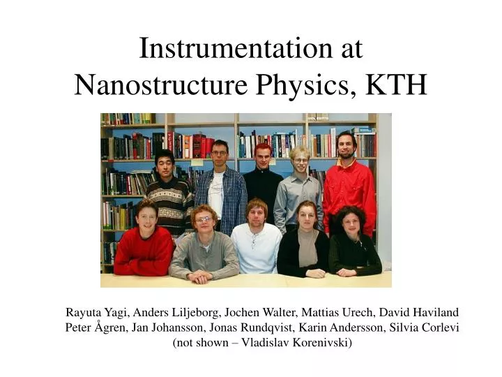
Instrumentation at Nanostructure Physics, KTH. Rayuta Yagi, Anders Liljeborg, Jochen Walter, Mattias Urech, David Haviland Peter Ågren, Jan Johansson, Jonas Rundqvist, Karin Andersson, Silvia Corlevi (not shown – Vladislav Korenivski). Our Realm in Experimental Physics. Low energies ( m eV)

E N D
Instrumentation at Nanostructure Physics, KTH Rayuta Yagi, Anders Liljeborg, Jochen Walter, Mattias Urech, David Haviland Peter Ågren, Jan Johansson, Jonas Rundqvist, Karin Andersson, Silvia Corlevi (not shown – Vladislav Korenivski)
Our Realm in Experimental Physics • Low energies (meV) • Low Temperatures (20 mK) • Small signals (nV, fA) • Single charge (2e=1.3x10⁻¹⁸ C) • Single flux quanta (F0=2.06x10⁻¹⁵ W m2) • Small dimensions (10 – 100 nm)
KTH Nano-Fab Lab Philosophy • Nano and micro scale fabrication,imaging and metrology • Joint laboratory facility, broad user spectrum • Graduate students are users • Low overhead costs, flexible research environment
K. A. Wallenberg Foundation • 9 Msek, 1998 • Electron-beam lithography • Plasma RIE • Wire bonder • clean benches, spinner, microscope, etc. • 10 Msek , 2001 • Atomic Force Microscope • Plasma RIE • Surface profilometer • photo lithography • clean benches
Low Cost (semi) clean room environment Phase 2 Instruments – Phase 1 Instruments Light Microscope Laminar flow benches (spinner, development) Photo Lithography Wet bench, hood Reactive Ion Etcher(s) Surface Profilometer Vacuum Deposition System E-beam lithography Atomic Force Microscope Wire Bonder Fluorescence Microscope Cooled CCD camera
Low cost clean (enough) environment500 – 2000 particles per cubic foot
Ventilated clean air hoodsparticle count < 1/ft.3 after 2 minutes
Electron beam lithography • Versatileresearch tool • Beam writing and SEM capability, 6 inch laser stage. • High resolution (slow, nano features) and Low Resolution (fast, micro structure) Raith Turnkey 150
Thickness measurement 0.1 Å vertical resolution 0.5 mm horizontal Low force (ca. mN?)
Scanning Probe Microscope • Nanoscope IV Multi-mode: • AFM (air, liquid) • STM (air) • MFM, ESFM etc. • Image surface • Force measurement
spin dependant transport in nano-scale junctions(Nanostructure Physics, KTH) Room Temperature Magneto-resistance (MR) Two closely spaced Co/AlOx/Co tunnel junctions
Superconducting nano-circuits as quantum bits(Nanostructure Physics, KTH; Quantum Field Theory, SU) Gate SQUID Au lead SET electrometer Al Tunnel junction
Nanostructured ferroelectrics for linear and nonlinear optics(Laser physics and quantum optics, KTH) Photonic Bandgap Structures ion-exchanged gratings in KTP • = 800 nm, depth > 200 m • aspect ratio > 500:1 • L= 2 mm, w=1mm used as passive narrow band filters Active devices – electrically addressable filters sub-micron periodically domain inverted structures fabricated for first time • = 720 nm, depth 500 m • aspect ratio > 500:1 • L=1 mm, W= 1 mm Top view Bottom view
Nano fabricated X-ray lenses(Biomedical and X-ray Physics, KTH) Compact X-ray Microscope Diffractive Optics -- Zone Plate
Nano-patterned surfaces for cell growth studies(Polymer Chemistry, KTH; Nanostructure Physics, KTH) Electron-microscope image Optical microscope image Sine-wave grooves in PMMA
S-H Protein A cys - biotin - neutravidin fluoro spheres self assemble on nanometer scale pattern(Nanostructure physics, KTH, Protein Engineering, KTH) Neutravidin 40 nm fluorescent sphere 10 mm PEG 50 Å Au 2000 Å
Measurement Equipment • Low Temperatures (down to 20 mk) • High Frequency (up to 2 GHz) • Small Signals (fA, nV, Lockin, low noise AF) • High Impedence (> G Ohm)
Low Temperature Dilution Refrigerator (Tmin 250 mK) He3 Crostat (Tmin 250 mK)
Low Frequency techniques • Lockin Amplifier • Low noise preamplifiers • Home-made based on BB OPA111, high source impedence, high CMR, symmetric baising circuit. • Standford 560 (voltage) and 570 (current) preamps • Noise Matching – match source impedance to input impedence of preamp at given frequency for minimum noise
Network Analyizer up to 2GHz Reflected and transmitted signal, Amplitude and phase • Impedance of high inductance microstrips • Permiability of magnetic films • Characterize transmission lines, couplings, filters No picture - Digital Sampling Oscilloscope with TDR module (ps resolution)
Vibrating Sample Magnetometer M vs. H of this magnetic films Also “loop tracer”, real time rotation in plane of film
Future HF Techniques • ns or sub-ns rise time pulses • Broadband cabling in to cryostat • CW generator greater than 2 GHz • AWF generator • Pulsed RF • Field calculations around microstrips • Tricks …. opto-electric? ……