Download
1 / 16
160 likes | 170 Vues
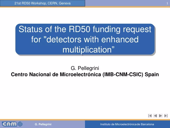
Status of the RD50 funding request for "detectors with enhanced multiplication”. G. Pellegrini Centro Nacional de Microelectrónica (IMB-CNM-CSIC) Spain. Old results. Trenched detectors with higher charge collection than standard after irradiation (w7 standard). Poly trench. Alibava Setup.

E N D
Status of the RD50 funding request for "detectors with enhanced multiplication” G. Pellegrini Centro Nacional de Microelectrónica (IMB-CNM-CSIC) Spain
Old results Trenched detectors with higher charge collection than standard after irradiation (w7 standard). Poly trench Alibava Setup CC(V) after 1E16 neq cm-2 • Anyway: • Trenches are not a standard process for detectors. • We need to have a controlled and understood multiplication. • Multiplication before irradiation is useful. • Trenches difficult the photolithography process, “pin holes” observed in the first batch. Rd50 funded project G. Casse, HSTD8, Taipei (TW) 4-7 Dec. 2011
Simulation of the Electric Field Standard Strip Strip with P-type diffusion Strip with P-type diffusion: 2D and 1D doping profiles
Simulation of the Electric Field High Electric Field peak at the junction Curves at 500 V Irradiated. Φeq = 1 x 10¹⁶ n/eq cm2 No Irradiated • Standard strip: electric field strength at the junction increases after irradiation • Strip with P-type diffusion: electric field strength at the junction is held after irradiation P. Fernandez et al, “Simulation of new p-type strip detectors with trench to enhance the charge multiplication effect in the n-type electrodes”
Mask layout Without p+ implantation With p+ implantation Round diode do not have p+ implantation
New run fabricated at CNM Marta Baselga
Charge Multiplication- pixel detectors We are proposing the fabrication of new p-type pixel detectors with enhanced multiplication effect in the n-type electrodes. 3 different approaches: • Thin p-type epitaxyal substrates • Low gain avalanche detectors • 3D with enhanced electric field. Status: approving of the mask and submission of the proposal to RD50 Same mask
1) Thin p-type epitaxyal substrates Detector proposed by Hartmut Sadrozinski and Abe Seiden (UCSC) , Ultra-Fast Silicon Detectors (UFSD). Provide in the same detector and readout chain • Ultra-fast timing resolution [10’s of ps] • Precision location information [10’s of µm] We propose to achieve high electric field is to use thin p-type epitaxyal substrates [1] grown on thick support wafers, p+-type doped, that acts as the backside ohmic contact. Different thicknesses will be used to study the multiplication effect induced by the high electric field at the collecting electrodes, depending on availability we propose to use: 10, 50, 75µm. Need very fast pixel readout. H. Sadrozinski, “Exploring charge multiplication for fast timing with silicon sensors” 20th RD50 Workshop, Bari 2012
2)Low gain avalanche detectors (LGAD) N+ Crating an n++/p+/p- junction along the centre of the electrodes. Under reverse bias conditions, a high electric field region is created at this localised region, which can lead to a multiplication mechanism. Standard FZ HR p-type wafers. P 285 um High Electric Field region leading to multiplication
3) 3D with enhanced electric field Simulation has shown that using silicon substrates with a resistivity <500ohm*cm could induce charge multiplication at low bias voltage but still depleting the detector bulk. We are ready to start the production on SOI p-type wafers (resistivity 100ohm*cm) with a thickness of 50µm to fabricate 3d thin detectors with medium or low multiplication factors before irradiations. J.P Balbuena, Simulation of 3D detectors, 6th Trento Workshop on Advanced Radiation Detectors, 2-4 March 2011 FBK, Povo di Trento, Italy
Mask design (planar) 6 AC strips 4 DC strips 4 FE-I4 8 FE-I3 7 pads 7 pads with multipl. Strip pitch 80um Marta Baselga
Detail of the mask P-stop 9um P-implant n-implant 2.5um Al
Conclusion • Strip detectors with p-implant must be tested before irradiation to measure multiplication. • Compare simulation with fabrication • Approval of the new mask • Submission of the proposal to RD50. • Start fabrication of 3D run.