Download
1 / 21
540 likes | 2.52k Vues
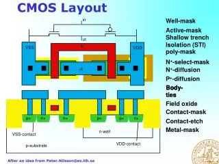
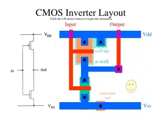
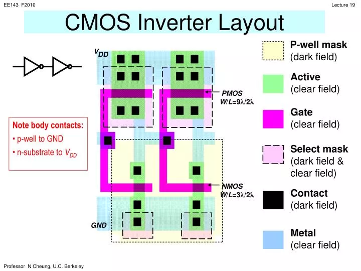
V. DD. CMOS Inverter Layout. P-well mask (dark field). Active (clear field). PMOS W / L =9 l /2 l. Gate (clear field). Note body contacts: p-well to GND n-substrate to V DD. Select mask (dark field & clear field). NMOS W / L =3 l /2 l. Contact (dark field). GND. Metal

E N D
V DD CMOS Inverter Layout P-well mask (dark field) Active (clear field) PMOS W/L=9l/2l Gate (clear field) • Note body contacts: • p-well to GND • n-substrate to VDD Select mask (dark field & clear field) NMOS W/L=3l/2l Contact (dark field) GND Metal (clear field)
Visualizing Layouts and Cross-Sections with SIMPLer • SIMPL is a CAD tool created by Prof. Neureuther’s group • allows IC designers to visualize device cross-sections • corresponding to a fabrication process and physical layout. • A Berkeley undergraduate student, Harlan Hile, created a mini-version of SIMPL (called SIMPLer) for EE40. • It’s a JAVA program -> can be run on any computer, • as well as on a web server. • A 3D version SIMPL-GL can be accessed at • http://cuervo2.eecs.berkeley.edu/Volcano/simpl_gl/main.htm
Form wells (implantation + thermal anneal) Grow gate oxide Deposit poly-Si and pattern gate electrodes Implant source/drain and body-contact regions Activate dopants (thermal anneal) Deposit insulating layer (SiO2); planarize (CMP) Open contact holes; deposit & pattern metal layer Twin Well + STI CMOS Process Define active areas; etch Si trenches Fill trenches (deposit SiO2 then CMP)
Well Engineering P-tub N-tub Twin Tub 10
Retrograde Well - formed by high energy (>200keV) implantation Conventional well (depth and profile controlled by diffusion drive-in) C(x) Retrograde well (depth and profile controlled by implantation energy and dose) x 12
Conventional vs Retrograde Well • Very low thermal budget for well formation • (no need for diffusion drive-in) • 2) Retrograde Well is formed AFTER field oxidation • small lateral diffusion and localized high conc under FOX 13
Example: Formation of Channel Stop and Retrograde Well in a single step Retrograde well Channel stop 14
Channel Engineering Shallow Oxide Trench Isolation
Self-Aligned Channel V-gate by Optical Lithography (SALVO) Process Smallest feature printable by lithography Normal S/D implant Oxide spacer poly-Si gate CVD oxide CVD oxide n+ n+ n+ n+ SiO2 Thermal gate oxide Angled Implant n+ pocket TiSi2 * Sub-50nm channels 19
SALVO Process Flow or See Homework Problem Chang et al, IEDM 2000 20
SUMMARY OF IC PROCESS INTEGRATION MODULE • Self aligned techniques: channel stop, Source/Drain, LDD, SALICIDE • How to read process flow descriptions and cross-sections • Generic NMOS Process with LOCOS • Generic CMOS Process with LOCOS and single well • Modified Processes: • Shallow Trench Isolation (STI), Twin Wells, Retrograde Well, SOI CMOS 21