Download

1 / 71
710 likes | 868 Vues
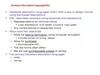
The Verilog Hardware Description Language. GUIDELINES. How to write HDL code:. GUIDELINES. How NOT to write HDL code:. Think Hardware NOT Software. Poorly written HDL code will either be: Unsynthesizable Functionally incorrect Lead to poor performance/area/power results. Conventions.

E N D
GUIDELINES • How to write HDL code:
GUIDELINES • How NOT to write HDL code:
Think Hardware NOT Software • Poorly written HDL code will either be: • Unsynthesizable • Functionally incorrect • Lead to poor performance/area/power results
Conventions • Verilog IS case sensitive • CLOCK, clock and Clock are different • Syntax is based on C • but is interpreted differently
Verilog code basic structure module module_name (ports); input input_signals; output output_signals; inout bidirectional signals; wire wire_signals; reg register_type_variables; primitive/component (ports); concurrent/sequential assignments endmodule
Port types • PORT DIRECTION - IN -OUT -INOUT • SIGNAL TYPE • scalar ( input x; ) • Vector (input [WIDTH -1 : 0] x)
Module port declaration example (1/2) module and_gate (o, i1, i2); output o; input i1; input i2; endmodule
Module port declaration example (2/2) module adder (carry, sum, i1, i2); output carry; output [3:0] sum; input [3:0] i1, i2; endmodule
Verilog Primitives • Verilog primitives are models of common combinational logic gates • Their functionality is built into the language and can be instantiated in designs directly • The output port of a primitive must be first in the list of ports
Structural description example module gates (o,i0,i1,i2,i3); output o; input i0,i1,i2,i3; wire s1, s2; and (s1, i0, i1); and (s2, i2, i3); and (o, s1, s2); endmodule
Verilog operators • Arithmetic +, - , *, Synthesizable /, % Non-synthesizable • Bitwise & AND | OR ~ NOT ^ XOR ~^ XNOR • Relational =, <, >, <=, >=
User-Defined Primitives Truth Table Models primitive my_UDP (y, x1, x2, x3); output y; //the output of a primitive cannot be a vector!! input x1, x2, x3; table //x1 x2 x3 : y 0 0 0 : 0; 0 0 1 : 1; 0 1 0 : 0; 0 1 1 : 0; 1 0 0 : 1; 1 0 1 : 0; 1 1 0 : 1; 1 1 1 : 0; endtable endprimitive
Truth tables with don’t cares table //? Represents a don’t care condition // on the input //i1 i2 i3 : y 0 0 0 : 0 0 0 1 : 1 0 1 0 : 0 0 1 1 : 0 1 ? ? : 1 endtable
variable assignment variable_name = value; //blocking assignment variable_name <= value; //non-blocking assignment Examples output a; output [6:0] b; reg [3:0] c; wire [2:0] d; CorrectIncorrect a = 1;a <= 3; b <= 7’b0101001; b = 9’b000011011; b[1] = 0; c <= 0; d <= 0; d <= {b , c}; b <= {c, d}; b[5:2] <= c;
Propagation delay Used to assign variables or primitives with delay, modeling circuit behaviour • # 5 and (s, i0, i1); -- 5 ns and gate delay • #5 assign s = i0 & i1; -- 5 ns and gate delay • #1 assign a = b; --1 ns wire delay Not synthesizable, is ignored by synthesis tools Useful in testbenches for creating input signal waveforms • always #20 clk = ~clk -- 40 ns clock period • #0 rst_n = 0; • #10 rst_n = 1;
Concurrent statements –delta time b = ~ a; (a = 1, b = 1, c =0) c = a ^ b; Time a b c 0 1 1 0 δ 1 0 0 2δ 1 0 1
Continuous assignment • Multiple driver error assign c = a & b; …. assign c = d | e;
Combinational circuit description module gates (d, a, c); output d; input a, c; //reg b; assign d = c ^ (~a); // assign b = ~a; // assign d = c ^ b; endmodule
Arithmetic unit description(full-adder) module add1 (cout, sum, a, b, cin); input a, b; input cin; output sum; output cout; assign {cout,sum} = a + b + cin; endmodule
Example Describe a 5-bit multiplier in Verilog.
Conditional assignment - describing MUXs assign = select_signal ? assignment1 : assignment1 module mux (o, s, i0, i1); output o; input i0, i1; input s; assign o = s ? i1 : i0; //if s =1 then o = i1, else o =i0 endmodule
Cyclic behavior • Statements in cyclic behavior execute sequentially • Can be used to describe either combinational circuits (optional) or sequential circuits (only way) always & (sensitivity list) begin sequential statements end
Combinational Circuit Description using Cyclic Behavior always @ (a or b or c) begin d = (a &b) |c; end ALL input signals must be in sensitivity list or latches will be produced!
If statement (sequential)– describing MUXs module mux (o, s, i0, i1); output o; reg o; input i0, i1; input s; always @ (i0 or i1 or s) begin if (s == 0) o = i0; else o = i1; end endmodule if (condition1) begin signal1 <= value1; signal2 <= value2; end else if (condition2) begin signal1 <= value3; signal2 <= value4; end … else begin signal1 <= valuen-1; signal2 <= valuen; end
CASE statement (sequential)– describing MUXs module mux (o, s, i0, i1); output o; reg o; input i0, i1; input s; always @ (i0 or i1 or s) begin case (s) 0: o = i0; 1: o = i1; default: o= 1’bx; endcase end endmodule case (signal) value1: signal1 <= value2; signal2 <= value3; value2 : signal1 <= value4; signal2 <= value5; . . . default: signal1 <= valuen-1; signal2 <= valuen; endcase
Example • Describe a 3-bit 4-to-1 MUX
CLOCKED PROCESS(Latch with asynchronous reset) always @ (clk or rst_n) begin if (rst_n == 0) q <= 0; else if (clk == 1) q <= d; end
CLOCKED PROCESS(Latchwith synchronous reset) always @ (clk or rst_n) begin if (clk == 1) q <= d; else if (rst_n == 0) q <= 0; end
CLOCKED PROCESS(Flip-flop with asynchronous reset) always @(posedge clk or negedge rst_n) begin if (rst_n == 0) q <= 0; else q <= d; end
CLOCKED PROCESS(Flip-flop with synchronous reset) always @(posedge clk) begin if (rst_n == 0) q <= 0; else q <= d; end
for loop statement – shift register module shift_reg (o, clk, rst_n, i); output o; input i; input clk, rst_n; reg [3:0] d; integer k; always @ (posedge clk or negedge rst_n) begin if (rst_n ==0) d <= 0; else begin d[0] <= i; for (k=0; k <2; k=k+1) d[k+1] <= d[k]; end end assign o = d[3]; endmodule
CLOCKED VS COMBINATIONAL PROCESS (1/2) always @ (posedge clk or negedge rst_n) begin if (rst_n == 0) q <= 0; else case (c) 0: q = a; 1: q = b; default: q= 1’bx; endcase end always @ (a or b or c) begin case (c) 0: q = a; 1: q = b; default: q= 1’bx; endcase end
CLOCKED VS COMBINATIONAL PROCESS (2/2) always @ (a or b or c) begin d = (a & b) | c; end always @ (posedge clk) begin if (rst_n == 0) d <= 0; else d <= (a & b) | c; end
EXAMPLE • DESCIBE A BINARY UP/DOWN COUNTER WITH ENABLE THAT COUNTS UPTO 12 AND THEN STARTS AGAIN FROM ZERO
TESTBENCH `timescale 1ns / 100ps module testbench_name (); reg ….; //declaration of register variables for DUT inputs wire …; //declaration of wires for DUT outputs DUT_name(DUT ports); initial $monitor(); //signals to be monitored (optional) initial begin #100 $finish; //end simulation end initial begin clk = 1’b0; //initialize clk #10 a = 0; #10 a = 1; … end always # 50 clk = ~clk; //50 ns clk period (if there is a clock) endmodule
TESTBENCH EXAMPLE `timescale 1ns / 100ps module mux_tb (); reg i0, i1, s; wire o; mux M1 (o, s, i0, i1); initial begin #100 $finish; //end simulation end initial begin //stimulus pattern #10 i0 = 0; i1=0; s=0; #10 i0=1; #10 i0 = 0; i1=1; #10 i0=1; #10 i0=0; i1= 0; s=1; #10 i0=1; #10 i0 = 0; i1=1; #10 i0=1; end endmodule
Mealy machines (1/5) module fsm (y, clk, rst_n, x); output y; input clk, rst_n, x; reg [1:0] state_pr, state_nx; reg y; parameter a = 0, b = 1, c = 2, d = 3, dont_care_state = 2’bx, dont_care_out = 1’bx;
Mealy machines (2/5) always @ (posedge clk or negedge rst_n) //state memory begin if (rst_n == 0) state_pr <= a; //default state else state_pr <= state_nx; end
Mealy machines (3/5) always @ (x or state_pr) //combinational part begin CASE (state_pr) a: if (x == 1) begin state_nx = b; y=0; end else if (x == 0) begin state_nx <= a; --optional y=0; end
Mealy machines (4/5) b: if (x == 1) begin state_nx = c; y=0; --Mealy machine end else if (x==0) begin state_nx <= a; y=0; --Mealy machine end c: if (x == 1) begin state_nx = c; --optional y=0; --Mealy machine end else if (x==0) begin state_nx <= d; y=0; --Mealy machine end
Mealy machines (5/5) d: if (x == 1) begin state_nx = b; y=1; --Mealy machine end else if (x==0) begin state_nx <= a; y=0; --Mealy machine end default: begin state_nx = dont_care_state; y <= dont_care_out; end endcase end endmodule
Moore machines always @ (x or state_pr) --combinational part begin CASE (state_pr) s0: y = <value>; --Moore machine if (x == 1) state_nx = s1; else state_nx = s0; --optional
MOORE MACHINES S1: y = <value>; --Moore machine if (x == 1) state_nx = S0; else state_nx = S1; --optional endcase end
EXAMPLE: OUT-OF-SEQUENCE COUNTER • DESCRIBE A COUNTER WITH THE FOLLOWING SEQUENCE: • “000” => “010” => “011” => “001” => “111” => “000”
ROM description (1/2) module rominfr (data, en, addr); output [3:0] data; input en; input [4:0] addr; reg [3:0] ROM [31:0]; assign data = ROM[addr];
ROM description (2/2) initial begin ROM[0] = 4’b0001; ROM[1] = 4’b0010; ROM[2] = 4’b0011; ROM[3] = 4’b0100; ROM[4] = 4’b0101; ROM[5] = 4’b0110; ROM[6] = 4’b0111; ROM[7] = 4’b1000; ROM[8] = 4’b1001; ROM[9] = 4’b1010; ROM[10] = 4’b1011; ROM[11] = 4’b1100; ROM[12] = 4’b1101; ROM[13] = 4’b1110; ROM[14] = 4’b1111; ROM[15] = 4’b0001; ROM[16] = 4’b0010; ROM[17] = 4’b0011; ROM[18] = 4’b0100; ROM[19] = 4’b0101; ROM[20] = 4’b0110; ROM[21] = 4’b0111; ROM[22] = 4’b1000; ROM[23] = 4’b1001; ROM[24] = 4’b1010; ROM[25] = 4’b1011; ROM[26] = 4’b1100; ROM[27] = 4’b1101; ROM[28] = 4’b1110; ROM[29] = 4’b1111; ROM[30] = 4’b0000; ROM[31] = 4’b0001; end endmodule