Download
1 / 38
380 likes | 728 Vues
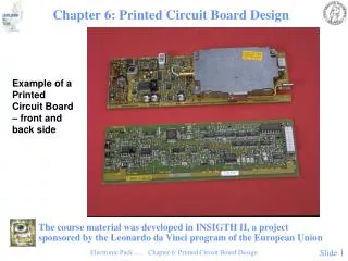
Introduction to CMOS VLSI Design Lecture 16: Circuit Pitfalls. David Harris Harvey Mudd College Spring 2004. Outline. Circuit Pitfalls Detective puzzle Given circuit and symptom, diagnose cause and recommend solution All these pitfalls have caused failures in real chips Noise Budgets

E N D
Introduction toCMOS VLSIDesignLecture 16: Circuit Pitfalls David Harris Harvey Mudd College Spring 2004
Outline • Circuit Pitfalls • Detective puzzle • Given circuit and symptom, diagnose cause and recommend solution • All these pitfalls have caused failures in real chips • Noise Budgets • Reliability
Circuit 2:1 multiplexer Symptom Mux works when selected D is 0 but not 1. Or fails at low VDD. Or fails in SF corner. Bad Circuit 1 • Principle: • Solution:
Circuit 2:1 multiplexer Symptom Mux works when selected D is 0 but not 1. Or fails at low VDD. Or fails in SF corner. Bad Circuit 1 • Principle: Threshold drop • X never rises above VDD-Vt • Vt is raised by the body effect • The threshold drop is most serious as Vt becomes a greater fraction of VDD. • Solution:
Circuit 2:1 multiplexer Symptom Mux works when selected D is 0 but not 1. Or fails at low VDD. Or fails in SF corner. Bad Circuit 1 • Principle: Threshold drop • X never rises above VDD-Vt • Vt is raised by the body effect • The threshold drop is most serious as Vt becomes a greater fraction of VDD. • Solution: Use transmission gates, not pass transistors
Circuit Latch Symptom Load a 0 into Q Set f = 0 Eventually Q spontaneously flips to 1 Bad Circuit 2 • Principle: • Solution:
Circuit Latch Symptom Load a 0 into Q Set f = 0 Eventually Q spontaneously flips to 1 Bad Circuit 2 • Principle: Leakage • X is a dynamic node holding value as charge on the node • Eventually subthreshold leakage may disturb charge • Solution:
Circuit Latch Symptom Load a 0 into Q Set f = 0 Eventually Q spontaneously flips to 1 Bad Circuit 2 • Principle: Leakage • X is a dynamic node holding value as charge on the node • Eventually subthreshold leakage may disturb charge • Solution: Stabilize node with feedback • Or periodically refresh node (requires fast clock, not practical processes with big leakage)
Circuit Domino AND gate Symptom Precharge gate (Y=0) Then evaluate Eventually Y spontaneously flips to 1 Bad Circuit 3 • Principle: • Solution:
Circuit Domino AND gate Symptom Precharge gate (Y=0) Then evaluate Eventually Y spontaneously flips to 1 Bad Circuit 3 • Principle: Leakage • X is a dynamic node holding value as charge on the node • Eventually subthreshold leakage may disturb charge • Solution:
Circuit Domino AND gate Symptom Precharge gate (Y=0) Then evaluate Eventually Y spontaneously flips to 1 Bad Circuit 3 • Principle: Leakage • X is a dynamic node holding value as charge on the node • Eventually subthreshold leakage may disturb charge • Solution: Keeper
Circuit Pseudo-nMOS OR Symptom When only one input is true, Y = 0. Perhaps only happens in SF corner. Bad Circuit 4 • Principle: • Solution:
Circuit Pseudo-nMOS OR Symptom When only one input is true, Y = 0. Perhaps only happens in SF corner. Bad Circuit 4 • Principle: Ratio Failure • nMOS and pMOS fight each other. • If the pMOS is too strong, nMOS cannot pull X low enough. • Solution:
Circuit Pseudo-nMOS OR Symptom When only one input is true, Y = 0. Perhaps only happens in SF corner. Bad Circuit 4 • Principle: Ratio Failure • nMOS and pMOS fight each other. • If the pMOS is too strong, nMOS cannot pull X low enough. • Solution: Check that ratio is satisfied in all corners
Circuit Latch Symptom Q stuck at 1. May only happen for certain latches where input is driven by a small gate located far away. Bad Circuit 5 • Principle: • Solutions:
Circuit Latch Symptom Q stuck at 1. May only happen for certain latches where input is driven by a small gate located far away. Bad Circuit 5 • Principle: Ratio Failure (again) • Series resistance of D driver, wire resistance, and tgate must be much less than weak feedback inverter. • Solutions:
Circuit Latch Symptom Q stuck at 1. May only happen for certain latches where input is driven by a small gate located far away. Bad Circuit 5 • Principle: Ratio Failure (again) • Series resistance of D driver, wire resistance, and tgate must be much less than weak feedback inverter. • Solutions: Check relative strengths • Avoid unbuffered diffusion inputs where driver is unknown
Circuit Domino AND gate Symptom Precharge gate while A = B = 0, so Z = 0 Set f = 1 A rises Z is observed to sometimes rise Bad Circuit 6 • Principle: • Solutions:
Circuit Domino AND gate Symptom Precharge gate while A = B = 0, so Z = 0 Set f = 1 A rises Z is observed to sometimes rise Bad Circuit 6 • Principle: Charge Sharing • If X was low, it shares charge with Y • Solutions:
Circuit Domino AND gate Symptom Precharge gate while A = B = 0, so Z = 0 Set f = 1 A rises Z is observed to sometimes rise Bad Circuit 6 • Principle: Charge Sharing • If X was low, it shares charge with Y • Solutions: Limit charge sharing • Safe if CY >> CX • Or precharge node X too
Circuit Dynamic gate + latch Symptom Precharge gate while transmission gate latch is opaque Evaluate When latch becomes transparent, X falls Bad Circuit 7 • Principle: • Solution:
Circuit Dynamic gate + latch Symptom Precharge gate while transmission gate latch is opaque Evaluate When latch becomes transparent, X falls Bad Circuit 7 • Principle: Charge Sharing • If Y was low, it shares charge with X • Solution:
Circuit Dynamic gate + latch Symptom Precharge gate while transmission gate latch is opaque Evaluate When latch becomes transparent, X falls Bad Circuit 7 • Principle: Charge Sharing • If Y was low, it shares charge with X • Solution: Buffer dynamic nodes before driving transmission gate
Circuit Latch Symptom Q changes while latch is opaque Especially if D comes from a far-away driver Bad Circuit 8 • Principle: • Solution:
Circuit Latch Symptom Q changes while latch is opaque Especially if D comes from a far-away driver Bad Circuit 8 • Principle: Diffusion Input Noise Sensitivity • If D < -Vt, transmission gate turns on • Most likely because of power supply noise or coupling on D • Solution:
Circuit Latch Symptom Q changes while latch is opaque Especially if D comes from a far-away driver Bad Circuit 8 • Principle: Diffusion Input Noise Sensitivity • If D < -Vtn, transmission gate turns on (same if D >VDD-Vtp) • Most likely because of power supply noise or coupling on D • Solution: Buffer D locally, so that GND and D have the same potential (or D and VDD)
Circuit Anything Symptom Some gates are slower than expected Bad Circuit 9 • Principle:
Circuit Anything Symptom Some gates are slower than expected Bad Circuit 9 • Principle: Hot Spots and Power Supply Noise
Noise • Sources • Power supply noise / ground bounce • Capacitive coupling • Charge sharing • Leakage • Noise feedthrough • Consequences • Increased delay (for noise to settle out) • Or incorrect computations
Reliability • Hard Errors • Soft Errors
Electromigration • “Electron wind” causes movement of metal atoms along wires • Excessive electromigration leads to open circuits • Most significant for unidirectional (DC) current • Depends on current density Jdc (current / area) • Exponential dependence on temperature • Black’s Equation: • Typical limits: Jdc < 1 – 2 mA / mm2
Self-Heating • Current through wire resistance generates heat • Oxide surrounding wires is a thermal insulator • Heat tends to build up in wires • Hotter wires are more resistive, slower • Self-heating limits AC current densities for reliability • Typical limits: Jrms < 15 mA / mm2
Hot Carriers • Electric fields across channel beget high energies in some carriers • These “hot” carriers may be blasted into the gate oxide where they become trapped • Accumulation of charge in oxide causes shift in Vt over time • Eventually Vt shifts too far for devices to operate correctly • Choose VDD to achieve reasonable product lifetime • Worst problems for inverters and NORs with slow input risetime and long propagation delays
Latchup • Latchup: positive feedback leading to VDD – GND short • Major problem for 1970’s CMOS processes before it was well understood • Avoid by minimizing resistance of body to GND / VDD • Use plenty of substrate and well taps
Guard Rings • Latchup risk greatest when diffusion-to-substrate diodes could become forward-biased • Surround sensitive region with guard ring to collect injected charge
Overvoltage • High voltages can damage transistors • Electrostatic discharge • Oxide arcing • Punchthrough • Time-dependent dielectric breakdown (TDDB) • Accumulated wear from tunneling currents • Requires low VDD for thin oxides and short channels • Use ESD protection structures where chip meets real world
Summary • Static CMOS gates are very robust • Will settle to correct value if you wait long enough • Other circuits suffer from a variety of pitfalls • Tradeoff between performance & robustness • Very important to check circuits for pitfalls • For large chips, you need an automatic checker. • Design rules aren’t worth the paper they are printed on unless you back them up with a tool.
Soft Errors • In 1970’s, DRAMs were observed to occasionally flip bits for no apparent reason • Ultimately linked to alpha particles and cosmic rays • Collisions with particles create electron-hole pairs in substrate • These carriers are collected on dynamic nodes, disturbing the voltage • Minimize soft errors by having plenty of charge on dynamic nodes • Tolerate errors through ECC, redundancy