Download
1 / 26
270 likes | 439 Vues
Optical properties of dielectric nanostructures. Motivation. Applications: Doped crystals lasers (radiation-resistant) Optical memory Difficulties of investigation. Content. Dielectrics Fluorites Quantum wells Nanostructures. Content. Dielectrics Fluorites Quantum wells

E N D
Motivation • Applications: • Doped crystals lasers (radiation-resistant) • Optical memory • Difficulties of investigation
Content Dielectrics Fluorites Quantum wells Nanostructures
Content Dielectrics Fluorites Quantum wells Nanostructures
Dielectrics • Non-conducting substance • “dia-electric” from Greek “dia” – “through” • No free charge carriers • Wide band gap > 5eV • Transparent in visible region • Ionic crystals • When doped exhibit semiconductor properties (CdF2)
Content Dielectrics Fluorites Quantum wells Nanostructures
Fluorites: lattice structure • Face-centered-cubic unit cell • Oh5 symmetry • The crystal is not piezoelectric • Close contact between different species of ions or atoms • Materials: • The halides: CaF2, CdF2, BaF2… • The oxides: ZrO2, CeO2… • The others… - Ca - F
Fluorites: energy-band structure Electronic configuration of ions • Main features: • Electron effective mass is comparable to free electron mass (0,5~1,0 m0) • The valence band: • Maximum is in Г-point • The conduction band: • Minimum is located in Г-point The energy bands of CaF2 Energy band formation
Fluorites: optical properties Energy band structure Transitions: Reflectance spectrum I III II
Content Dielectrics Fluorites Quantum wells Nanostructures
Quantum wells Eg1 Eg2 Energy levels for infinite well Selection rule
Content Dielectrics Fluorites Quantum wells Nanostructures
KCl-KBr Multilayer Quantum wells • Evaporation on to cleaved LiFsubstarate • Specimens: • SL2: KBr 100A-layer • C-ML: a double structure of KBr 100A on KCl 200A • D-ML: a triple structure of KBr 100A sandwiched by two KCl 200A • E-ML: a 3,5 periods one of KCl 150A – KBr 50A
KI-KBr and KI-KClMultilayers • Evaporation onto a quartz glass substrate • Specimens: • KI layer is sandwiched between KBr layer of the same thickness
KIx-KBr1-x mixed crystal films • Blue shifts: • Quantum confinement effects • Interlayer mixed crystallization
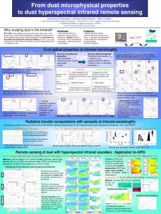
CaF2-CdF2heterostructures on Si Energy difference atthe interface CaF2/CdF2:2,9 eV in the conduction band1,2 eV in the valence band • Specimens: • 1: Si-CaF2(30ML)-CaF2 • 2: Si-CaF2-CdF2(10ML)-CaF2 • 3: Si-CaF2-CdF2(30ML)-CaF2 • 4: Si-CaF2-CdF2(90ML)-CaF2 • 5: Si-CaF2-6x[CaF2(5ML)-CdF2(5ML)]-CaF2 • 6: Si-CaF2-14x[CaF2(2,5ML)-CdF2(2ML)]-CaF2 • 7: Si-CaF2-3x[CaF2(10ML)-CdF2(10ML)]-CaF2 12.1eV 8eV Opposite sing of the fluoride lattice mismatch to Si flavors strain compensation and growth of pseudomorthic superlattices CaF2 CdF2 Lattice constants:CaF2 5,46 A0CdF2 5,39 A0Si 5,43 A0 Si CaF2 CaF2 CdF2 CaF2 CdF2 CaF2 CdF2 CaF2
To add transitions CaF2-CdF2heterostructures on Si CaF2-CdF2 10ML CaF2-CdF2 5ML CaF2-CdF2 2ML CaF2-CdF2 90ML CaF2-CdF2 30ML CaF2-CdF2 10ML CaF2
The harmonic oscillator model - complex dielectric constant - refractive index - reflection coefficient - reflectivity
CaF2 harmonic approximation • Oscillators parameters:
CaF2-CdF2heterostructures on Si • Future plans: • To calculate phase of reflective index • To calculate reflectance spectrum from thin films • To estimate energy level shifts in quantum well • To estimate interface effects
Nanoislands: low temperature growth • 1 CaF2 multilayer at 4500C • CaF2 nanoislands stretched along <110> direction • Bare Si surface between CaF2 islands
CaF2 stripes: high temperature growth • 6 CaF2 multilayers at 7000C • CaF2 stripes are aligned along <110> direction • Stripes length – several microns, height – 3-6 nm • Formation of wetting layer
MBE-growth of CaF2/CdF2superlattices X-Ray diffraction TEM 6ML 4ML 10ML T/2 High crystalline quality
The first Brillouin zone of the face-centered-cubic fluorite lattice