Download
1 / 64
640 likes | 775 Vues
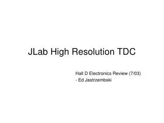
Development of a high performance TDC module for the Grapes-3 experiment. B.Satyanarayana Department of High Energy Physics. Next ASET Colloquium. Performance of the TDC module developed for the Grapes-3 experiment. S.Karthikeyan Department of High Energy Physics. The team.

E N D
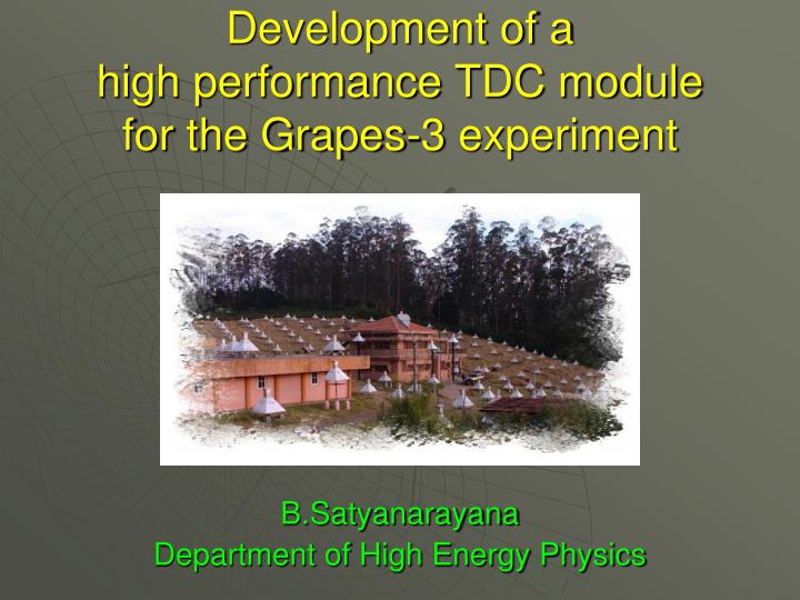
Development of ahigh performance TDC modulefor the Grapes-3 experiment B.Satyanarayana Department of High Energy Physics
Next ASET Colloquium Performance of the TDC module developed for the Grapes-3 experiment S.Karthikeyan Department of High Energy Physics
The team S.K.Gupta¶, Y.Hayashi§, A.Iyer¶, P.Jagadeesan¶, A.Jain¶, S.Karthikeyan¶, S.Kawakami§, K.C.Ravindran¶, B.Satyanarayana¶ and S.C.Tonwar¶ ¶Tata Institute of Fundamental Research, Mumbai, INDIA §Osaka City University, Osaka, Japan B.Satyanarayana, DHEP
Plan of the talk • Introduction to Time to Digital Converters • Grapes’ time measurement requirements • Specifications of the TDC32 ASIC • Functional blocks of TDC32 • Hardware design of the TDC module • JTAG interface designs • Deployment in the Grapes-3 experiment • Summary and outlook • Acknowledgements B.Satyanarayana, DHEP
Next topic of the talk • Introduction to Time to Digital Converters • Grapes’ time measurement requirements • Specifications of the TDC32 ASIC • Functional blocks of TDC32 • Hardware design of the TDC module • JTAG interface designs • Deployment in the Grapes-3 experiment • Summary and outlook • Acknowledgements B.Satyanarayana, DHEP
Start Stop Time scale (clock) Hits Why TDCs? TDCs are used to measure time or intervals • Start – Stop measurement • Measurement of time interval between two events: Start signal – Stop signal • Used to measure relatively short time intervals with high precision • Like a stop watch used to measure sport competitions • Time tagging • Measure time of occurrence of events with a given time reference: Time reference (Clock) Events to be measured (Hits) • Used to measure relative occurrence of many events on a defined time scale: Such a time scale will have limited range; like 12/24 hour time scale on your watch when having no date and year B.Satyanarayana, DHEP
Where TDCs? • Special needs for High Energy Physics • Many thousands of channels needed • Rate of measurements can be very high • Very high timing resolution • A mechanism to store measurements during a given interval and extract only those related to an interesting event, signaled by a trigger, must be integrated with TDC function • Other applications • Laser/radar ranging to measure distance between cars • Time delay reflection to measure location of broken fiber • Most other applications only needs one or a few channels B.Satyanarayana, DHEP
Pipelined TDC architecture • Stores hit data every clock cycle • High hit rates (one per clock cycle) • Fixed dead time; but limited double pulse resolution • Fixed trigger latency; limited by buffer size • Only useful in triggered mode • Difficult to support overlapping triggers • No problem with buffer occupancies • Narrow but deep latency buffer • Simple architecture; quick implementation • Limitedflexibility • Examples • LeCroy’s FASTBUS DC TDCs • DAQ of KGF underground experiments Small dynamic range (25ns) Hit Clock Synchronous trigger Output FIFO B.Satyanarayana, DHEP
Data driven TDC architecture • Only stores data when hit detected • Variable latency over full dynamic range • Compromise between hit rate and latency • Triggered/non triggered modes • Multiple overlapping triggers • Channel merging via de-randomizers;Limits hit rates • Good double pulse resolution;But complicated dead time analysis • Buffer occupancies must be seriously analyzed • Buffer overflows must be handled carefully • Hit may be lost if marked • Complete events must never be lost • Wide latency buffer (covers full dynamic range) • More complicated architecture/implementation • Logic complication handled by logic synthesis • Extended verifications at behavioral/register/gate level • High flexibility Large dynamic range Hit FIFO orDual port RAM Triggertime tag Trigger Latency - Compare time Output FIFO Derandomizer FIFO’s Common FIFO B.Satyanarayana, DHEP
Stop Start Clock Counter Start-stop type Cable delay chain Basic TDC types - I • Counter type • Advantages • Simple; but still useful! • Digital • large dynamic range possible • Easy to integrate many channels per chip • Disadvantages • Limited time resolution (1ns using modern CMOS technology) • Metastability (use of Gray code counter) • Single Delay chain type • Cable delay chain (distributed L-C) • Very good resolution (5ps mm) • Not easy to integrate on integrated circuits • Simple delay chain using active gates • Good resolution (~100ps using modern tech) • Limited dynamic range (long delay chain and register) • Only start-stop type • Large delay variations between chips and with temperature and supply voltage Reset Clock Counter Hit Register Time tagging type Delay chain with non-inverting gates Start Register Stop B.Satyanarayana, DHEP
Delay Locked Loop Phase Clock Hit Register R R R R C C C C RC delay chain V t Basic TDC types - II • Single Delay chain type (Contd…) • Delay locked loop • Self calibrating using external frequency reference (clock) • Allows combination with counter • Delicate feedback loop design (jitter) • R-C delay chain • Very good resolution • Signal slew rate deteriorates • Delay chain with losses; so only short delay chain possible • Large sensitivity to process parameters (and temperature) B.Satyanarayana, DHEP
Clock PD PD PD PD PD Start delay chain: Tstart Start D D D D D D D D Vernier principle Resolution: Tstart - Tstop Stop Stop delay chain: Tstop Basic TDC types - III • Multiple delay chain type • Vernier delay chain types • Resolution determined by delay difference between two chains. Delay difference can be made very small and very high resolution can be obtained. • Small dynamic range (long chains) • Delay chains can not be directly calibrated using DLL • Matching between delay cells becomes critical • Coupled delay locked loops • Sub-delay cell resolution (¼) • All DLLs use common time reference (clock) • Common timing generator for multiple channels • Jitter analysis not trivial T2 = T1 + Δ T1 Resolution: T2 – T1 = Δ B.Satyanarayana, DHEP
Start Stop ADC Start Stop Start Stop Stretched time Basic TDC types - IV • Charge integration • Using ADC (TAC) • High resolution • Low dynamic range • Sensitive analog design • Low hit rate • Requires ADC • Using double slope (time stretcher) • No need for ADC (substituted with a counter) • Multiple exotic architectures • Heavily coupled phase locked loops • Beating between two PLLs • Re-circulating delay loops • Summing of signals with different slew rates I1 Start Clock Disc. Stop Counter I2 = I1/k B.Satyanarayana, DHEP
How to compare TDCs? • Merits • Resolution • Bin size and effective resolution (RMS, INL, DNL) • Dynamic range • Stability • Use of external reference • Drift (e.g. temperature) • Jitter and Noise • Integration issues • Digital / analog • Noise / power supply sensitivity • Sensitivity to matching of active elements • Required IC area • Common timing block per channel • Time critical block must be implemented on chip together with noisy digital logic • Use in final system • Can one actually use effectively very high time resolution in large systems (detectors) • Calibration - stability • Distribution of timing reference (start signal or reference clock) • Other features: data buffering, triggering, readout, test, radiation, etc. B.Satyanarayana, DHEP
Next topic of the talk • Introduction to Time to Digital Converters • Grapes’ time measurement requirements • Specifications of the TDC32 ASIC • Functional blocks of TDC32 • Hardware design of the TDC module • JTAG interface designs • Deployment in the Grapes-3 experiment • Summary and outlook • Acknowledgements B.Satyanarayana, DHEP
Grapes’ TDC requirements • Many hundreds of channels needed • Low cost per channel • Considerations of the input signal type • Rate of measurements can be very high • Decent timing resolution • Trigger matching capability • Multi-hit facility preferable • High stability, low jitter and drift • Simple calibration procedure • Individual channel offsets/presets B.Satyanarayana, DHEP
Next topic of the talk • Introduction to Time to Digital Converters • Grapes’ time measurement requirements • Specifications of the TDC32 ASIC • Functional blocks of TDC32 • Hardware design of the TDC module • JTAG interface designs • Deployment in the Grapes-3 experiment • Summary and outlook • Acknowledgements B.Satyanarayana, DHEP
The TDC32 ASIC chip Chip designer JÖrgen Christiansen ECP-MIC Microelectronics Group CERN, Geneva Prominent users LHC, ALICE, CMS, ATLAS, BES, NA48, STAR, CAEN etc. 84-pin PLCC B.Satyanarayana, DHEP
Specifications of the TDC32 ASIC • Number of channels: 32 + 1 Common start • Clock frequency: 20-60MHz • Time bin size: 520ps @60MHz • DNL: ±130ps(max), 63ps(RMS) @60MHz • INL: ±280ps(max), 130ps(RMS) @60MHz • Time resolution: 200ps(RMS) @60MHz • Difference between channels: One time bin (max) • Variation with temperature: One time bin (max) • Dynamic range: 21 bits • Double pulse resolution: 15ns • Max recommended hit rate: 750KHz per channel • Event buffer size: 256 • Read-out buffer size: 32 • Trigger buffer size: 8 • Power supply: 4.75-5.25Volts, ~100mA @60MHz • Temperature range: -40 to 80o C • Hit input threshold voltage: Standard TTL B.Satyanarayana, DHEP
Next topic of the talk • Introduction to Time to Digital Converters • Grapes’ time measurement requirements • Specifications of the TDC32 ASIC • Functional blocks of TDC32 • Hardware design of the TDC module • JTAG interface designs • Deployment in the Grapes-3 experiment • Summary and outlook • Acknowledgements B.Satyanarayana, DHEP
Architecture of TDC32 B.Satyanarayana, DHEP
Delay Locked Loop • Three major components: • Chain of 32 delay elements; adjustable delay • Phase detector between clock and delayed signal • Charge pump & level shifter generating control voltage to the delay elements • Jitter in the delay chain • Lock monitoring • Dynamics of the control loop • Programmable charge pump current level B.Satyanarayana, DHEP
Coarse time count • Dynamic range of the fine time measurement, extracted from the state of DLL is expanded, by • Storing the state of a clock synchronous counter • Hit signal is synchronous to the clocking, so • Two count values, ½ a clock cycle out of phase stored • At reset, coarse time counter loaded with time offset B.Satyanarayana, DHEP
Hit registers • Programmable edge (rising or falling) detection • De-glitched hit signal is used to load a timing register • Individual channels can be enabled or disabled • Self timed controller based double timing registers • De-randomisation; double synchronisers B.Satyanarayana, DHEP
Channel offset adjustment • Variable detector-to-control room distances and thus cable lengths • Coaxial cable – Astronomer's best choice for signal delay adjustment, but a costly one! • Common programmable coarse time count offset • Individual programmable fine time adjustment possible • Eight bit (3 bits coarse, 5 bits fine) channel dependent constant • Stored in a 32 words by 8 bits wide memory B.Satyanarayana, DHEP
Start-Stop timing • Start time measurement done by a dedicated channel • Start channel is just a superior priority channel • Start time transferred to the register on hit - immediately • Previous data must therefore be stored before next start • Start time can be subtracted from all hits • Start signal can gate all the stops; used in Grapes’ modules Common start time subtraction Start gating B.Satyanarayana, DHEP
Event buffer • 256 hits deep circular buffer • Coarse and fine time counts + Channel id + Time tag • Channel arbitration schemes • Reading is random access • Trigger matching can search for data belonging to the received triggers • Write pointer never overtakes read pointer • Error flagged if the event buffer overflows • Hits data lost only if both primary and secondary registers are full B.Satyanarayana, DHEP
Trigger matching • Time match between trigger time tag and stops • Hits matching trigger pushed to readout FIFO • Trigger time tag can be subtracted from all stops – bunch crossing • Global time reference – t0 – time since TDC RESET • Trigger matching within a programmable window • Allowed trigger latency 32768 clock periods • Hits are not written in strict temporal order • A hit may belong to several closely spaced triggers • Two search pointers and two programmable windows used B.Satyanarayana, DHEP
Trigger interface • Trigger matching based on trigger tag locating in time where hits belong to an event of interest • Trigger tags pushed into 8-word deep trigger FIFO • Several ways of supplying trigger time tags • Parallel transfer via readout bus • Serial transfer • Centrally loading time tag counter into a register B.Satyanarayana, DHEP
Readout FIFO • 32 words deep • Enable one event to be readout, while another is being processed • If readout FIFO runs full, the trigger matching process stops • Event separators if trigger matching enabled; effective readout FIFO size reduced B.Satyanarayana, DHEP
Readout interface • Readout via clock synchronous bus • Several TDCs may share a bus • Event synchronised readout if trigger matching enabled using Event_end and Next_event handshake • Readout of individual hits using Data_ready and Get_data handshake • Readout at TDC’s full speed if Get_data held HIGH • Low speed readout via Data_ready and Get_data handshake • Token based readout protocol for multiple chip boards B.Satyanarayana, DHEP
JTAG registers JTAG instruction register (4) Boundary scan register (89) Setup registers (127) Control registers (33) Status registers (5) Internal status registers (59) JTAG instructions EXTEST: Boundary scan for inter-chip connections IDCODE: Read 32-bit chip ID code SAMPLE: Sample of all chip pins INTEST: Use boundary scan registers to test the chip SETUP: Load of setup data CONTROL: Load of control information STATUS: Read of status information CORETEST: Access to internal test scan registers BYPASS: Bypass the chip in a cascade JTAG test and programming port • Joint Test Action Group (JTAG) • Standard IEEE 1149.1 • Used to setup programmable features • Get access to test facilities built into the chip B.Satyanarayana, DHEP
[15:0] Yes/No trigger time tag offset [16] Enable parallel trigger [17] Enable synchronous trigger [18] Enable Serial trigger [34:19] Trigger matching window [35] Enable readout of start measurements [36] Enable subtraction of trigger time tag [37] Enable overlapping triggers [45:38] Looking back window [7:0] [53:46] Looking forward window [7:0] [54] Enable subtraction of start time [55] Enable matching [56] Enable automatic reject [72:57] Reject offset [15:0] [78:73] Adjust channel offset [5:0] [86:79] Adjust common offset [7:0] [87] Enable individual adjust [89:88] Operating mode: 00 = normal [94:90] DLL current level [95] DLL reset [96] Detect falling edge start [97] Detect falling edge odd channels [98] Detect falling edge even channels [99] Detect both edges (all channels) [100] Enable empty start [101] Must be equal to setup [54] [102] Enable double synchronisers [103] Enable double hit priority queue [104] Enable start gating [120:105] Coarse count offset [121] Enable token read-out mode [122] Not locked error mask [123] Hit error error mask [124] Event buffer overflow error mask [125] Trigger buffer overflow error mask [126] Serial trigger error error mask JTAG setup register fields B.Satyanarayana, DHEP
TDC reset • Main reference of the TDC is clock • Synchronous TDC Reset defines T0 • DLL is not reset when Reset pin of the TDC asserted; must be done via JTAG interface • All buffers, counters and state machines are initialised on reset to their default values • Needs to be done only at startup B.Satyanarayana, DHEP
Error and status flags • All main functional blocks are continuously monitored for error conditions • Error state of individual parts can only be accessed via JTAG status scan path • Error flags supported • (DLL) Not_locked • Hit_error (while writing to event buffer) • Event_buffer_overflow • Trigger_buffer_overflow • Serial_trigger_error • All but the Not_locked error cleared by Reset • A general purpose error pin can be programmed to signal the error conditions needed B.Satyanarayana, DHEP
Next topic of the talk • Introduction to Time to Digital Converters • Grapes’ time measurement requirements • Specifications of the TDC32 ASIC • Functional blocks of TDC32 • Hardware design of the TDC module • JTAG interface designs • Deployment in the Grapes-3 experiment • Summary and outlook • Acknowledgements B.Satyanarayana, DHEP
Block diagram of the TDC module Power B.Satyanarayana, DHEP
TDC module: Input section B.Satyanarayana, DHEP
TDC module: Core section B.Satyanarayana, DHEP
TDC module: Control section B.Satyanarayana, DHEP
TDC module: CAMAC section B.Satyanarayana, DHEP
TDC module: JTAG section B.Satyanarayana, DHEP
TDC module: Power supplies B.Satyanarayana, DHEP
What had begun like this … B.Satyanarayana, DHEP
… ended like this B.Satyanarayana, DHEP
Next topic of the talk • Introduction to Time to Digital Converters • Grapes’ time measurement requirements • Specifications of the TDC32 ASIC • Functional blocks of TDC32 • Hardware design of the TDC module • JTAG interface designs • Deployment in the Grapes-3 experiment • Summary and outlook • Acknowledgements B.Satyanarayana, DHEP
Schematics of JTAG controllers 1 MHz NIM module PC Printer port B.Satyanarayana, DHEP
Next topic of the talk • Introduction to Time to Digital Converters • Grapes’ time measurement requirements • Specifications of the TDC32 ASIC • Functional blocks of TDC32 • Hardware design of the TDC module • JTAG interface designs • Deployment in the Grapes-3 experiment • Summary and outlook • Acknowledgements B.Satyanarayana, DHEP
Deployment in Grapes-3 • Module supports standard CAMAC as well as Grapes’ CAMAC interfaces • Module tested with 20, 40 and 60MHz clocks using a sophisticated custom built TDC calibration system • First module installed in the experiment using Start-Stop mode in December 2003; parallel readout along with a Phillips Scientific module for comparison • Second module installed in April 2004 using trigger matching mode; got rid of 80m/channel coaxial cables! • Module with improved PCB installed in January 2005 • Supports both Start-stop and trigger matching modes • CAMAC interface packed in an iSPL chip • Currently three modules in the system and two more waiting for their turn • In-situ calibration scheme used for rigorous monitoring B.Satyanarayana, DHEP
Next topic of the talk • Introduction to Time to Digital Converters • Grapes’ time measurement requirements • Specifications of the TDC32 ASIC • Functional blocks of TDC32 • Hardware design of the TDC module • JTAG interface designs • Deployment in the Grapes-3 experiment • Summary and outlook • Acknowledgements B.Satyanarayana, DHEP