Download

1 / 17
190 likes | 580 Vues
MOSFET Metal Oxide Semiconductor Field Effect Transistor. Introduction. It is a type of transistor Another name for the MOSFET is the insulated-gate FET or IGFET. This name emphasizes the fact that the gate electrode is electrically insulated from the device body (by the oxide layer).

E N D
Introduction • It is a type of transistor • Another name for the MOSFET is the insulated-gate FET or IGFET. • This name emphasizes the fact that the gate electrode is electrically insulated from the device body (by the oxide layer). • It is this insulation that causes the current in the gate terminal to be extremely small (of the order of (10 -15 A).
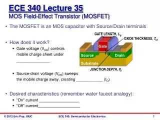
Device Structure • The transistor is fabricated on a p-typesubstrate, which is a single-crystal silicon wafer that provides physical support for the device. Two heavily doped n-type regions, indicated in the figure as the n+ source and the n+ drain regions, are created in the substrate. • A thin layer of silicon dioxide (Si02) of thickness tox(typically 2-50nm)2, is grown on the surface of the substrate, covering the area between the source and drain regions. • Metal is deposited on top of the oxide layer to form the gate electrode of the device. Metal contacts are also made to the source region, the drain region, and the substrate, also known as the body.
Four terminals are brought out: the gate terminal (G), the source terminal (S), the drain terminal (D), and the substrate or body terminal (B).
Device Operation • The source and the drain have been grounded and a positive voltage is applied to the gate. Since the source is grounded, the gate voltage appears in effect between gate and source and thus is denoted vGS. • The positive voltage on the gate causes the free holes to be repelled from the region of the substrate under the gate (the channel region). These holes are pushed downward into the substrate, leaving behind a carrier-depletion region. The depletion region is populated by the bound negative charge associated with the acceptor atoms.
The positive gate voltage attracts electrons from the n+ source and drain regions into the channel region. When a sufficient number of electrons accumulate near the surface of the substrate under the gate, an nregion is in effect created, connecting the source and drain regions. • Now if a voltage is applied between drain and source, current flows through this induced nregion, carried by the mobile electrons. The inducednregion thus forms a channel for current flow from drain to source.
This induced channel is also called an inversion layer. • The value of vGS at which a sufficient number of mobile electrons accumulate in the channel region to form a conducting channel is called the threshold voltage and is denoted Vt.
Now applying a positive voltage vDSbetween drain and source. The voltage vDScauses a current iDto flow through the induced n channel. Current is carried by free electrons traveling from source to drain. • The magnitude of iDdepends on the density of electrons in the channel, which in turn depends on the magnitude of vGS . • Specifically, for vGS = Vtthe channel is just induced and the current conducted is still negligibly small. As vGSexceeds Vtmore electrons are attracted into the channel. The result is a channel of increased conductance or, equivalently, reduced resistance. • The conductance of the channel is proportional to the excess gate voltage(vGS- Vt), also known as the effective voltage or the overdrive voltage.
Operation as vDSIs Increased • let vGSbe held constant at a value greater than Vt and vDSappears as a voltage drop across the length of the channel. That is, as we travel along the channel from source to drain, the voltage increases from 0 to vDS. Thus the voltage between the gate and points along the channel decreases from vGSat the source end to vGS - vDSat the drain end. Since the channel depth depends on this voltage the channel is now no longer of uniform depth; rather, the channel will take the tapered form, being deepest at the source end and shallowest at the drain end. • As vDSis increased, the channel becomes more tapered and its resistance increases correspondingly. Eventually, when vDSis increased to the value that reduces the voltage between gate and channel at the drain end to Vtthat is, vGD = Vtor vGS - vDS = Vtor vDS = vGS - Vtthe channel depth at the drain end decreases to almost zero, and the channel is said to be pinched off.
Increasing vDSbeyond this value has little effect (theoretically, no effect) on the channel shape, and the current through the channel remains constant at the value reached for vDS - vGS - Vt .The drain current thus saturates at this value, and the MOSFET is said to have entered the saturation region of operation. The voltage vDSat which saturation occurs is denoted vDSsat • VDSsat = VGS - Vt • The region of the iD-vDScharacteristic obtained for vDS < vDSsatis called the triode region
iD - vDSRelationship Where k'n is the process transconductance parameter The drain current is proportional to the ratio of the channel width W to the channel length L, known as the aspect ratio of the MOSFET
Resistor Loaded NMOS Inverter • The input to the inverter is at the gate of the N-channel output transistor NO and VIN = VGS. The output is at the drain and VOUT = VDS = VDD – IRL RL. For VIN < Vt, transistor is in cut off mode and does not conduct drain current. Since the ID(OFF) = 0 and the output is VOUT = VDD. As the input is increased slightly above the threshold voltage transistor begins to conduct. At this point only a small current flows and the drain voltage is lightly less than VDD. • As long as VDS >= VGS – Vt, transistor is operating in the saturation region. With further increase of the input, a larger drain current conducts and the output voltage continues to fall. • In summary, for a low input the output is high. Conversely for a high input the output is low.