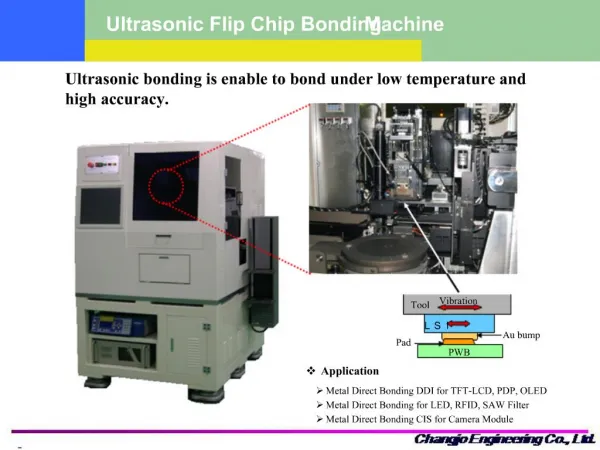
Download
1 / 90
970 likes | 1.38k Vues
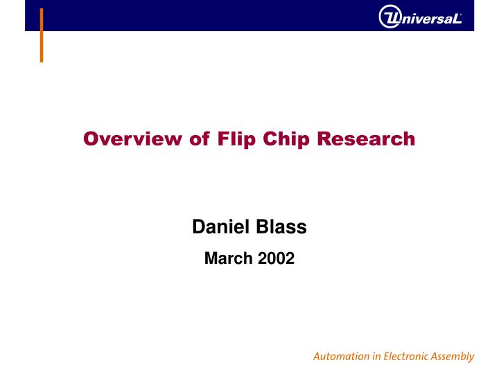
Overview of Flip Chip Research. Daniel Blass March 2002. Assembly. Lead-Free Assembly Flip Chip in Air Flux Jetting of Liquid No-Clean Fluxes Flip Chip on Flex Reflow Encapsulants Substrate Characterizations Information Needed For Yield Predictions Assembly Yield Software.

E N D
Overview of Flip Chip Research Daniel Blass March 2002
Assembly • Lead-Free Assembly • Flip Chip in Air • Flux Jetting of Liquid No-Clean Fluxes • Flip Chip on Flex • Reflow Encapsulants • Substrate Characterizations • Information Needed For Yield Predictions • Assembly Yield Software
Underfilling • Self-Filleting • Solder Extrusions & Trench Solder Mask Openings • Underfill Flow Modeling • Transfer Molding • No Void-Free Process Yet • Reflow Encapsulant Codification • Process Cook-Book / Guide • Underfilling Codification
Reliability • Moisture and Aging • Fillet Cracking Experiments • Crack Growth Experiments and Modeling • Lead-Free Reliability • Pad Finish • Reflow Attach Profile • Additional Reflows/JEDEC Level 3 Test • Transfer Molded Flip Chips • Results Comparable to a Capillary Flow Underfill
High Temp JEDEC Level 3 Testing • Moisture/Reflow Sensitivity Classification for Nonhermetic Solid State Surface Mount Devices • Component Qualification Test • Moisture Load Parts and Reflow 3 Times • Most Lead-Free Alloys Require Much Hotter Reflow Temperatures • Qualify to Higher Reflow Temperatures
Lead-Free Assembly • LF-2 (Sn95.5Ag3.5Cu1.0) from K&S Flip Chip • Liquidus of Approx. 217°C • Previous Process Recommendations • Dip in 2.0 mil of Kester TSF-6522 Flux • Nitrogen Reflow Atmosphere (50 ppm O2) • Peak Reflow Temperature of 238°C to 245°C • 50 to 70 Seconds Above 217°C • Soldering to Ni/Au or Cu-OSP Pads (Entek Plus) • This Process, However, Has Not Given Consistent Defect-Free Assembly • Incomplete Wetting of Pad, Poor Self-Centering • Only One Electrical Open (on Cu-OSP Pads)
Better Soldering to Ni/Au Pads • 250+ Chips On Each Pad Finish
Most LF-2 Chips Attached to Ni/Au Pads Had No Defects • 250+ Chips On Each Pad Finish
Sample Sizes with Each Process Largest Sample Sizes Built With Profile B or Profile G & 2 mil Kester TSF-6522
Average Defects Per Chip on Each Ni/Au Board Built With Profile B or G & 2 mil of Kester TSF-6522 Flux
Average Defects Per Chip on Each Cu-OSP Board Built With Profile B or G & 2 mil of Kester TSF-6522 Flux
Large Variation Within Each Process • Limits Ability to Compare Processes that Have Smaller Sample Sizes • Would Have to Build Many More Die To Decide Whether a Reflow Profile Was Better • All Processes Gave Soldering Defects
Thicker Flux Often Gave More Defects • Real Effect or Just Small Sample Sizes? • Good that 1.5 mil of Flux Is Not Worse
Future Direction of Lead-Free Assembly • New “Lead-Free” Fluxes • Heraeus TF69 • Not Suitable for Drum Fluxer: Large Solid Particles • Indium TAC 23 • Kester R903 • Have Not Eliminated Soldering Defects • Flux-Jetting of Liquid No-Clean Fluxes
Future Direction of Lead-Free Assembly • Alternative Finishes • Cu / Omikrontm Immersion White Tin • Cu / AlphaLEVELtm Organo-Metallic Immersion Silver • Electroless Ni / Immersion Silver (ENIS) • Would Likely to Have Same Reliability Issues as Electroless Ni / Immersion Au (ENIG) • Reflow Profile Optimization • Other Alloys? • Limited Soldering Trials with Sn/Ag/Bi • Interest?
Lead-Free Reflow Profiles • Profile Optimization • Lower Soak Temp • Shorter Soak or No Soak • Sharper Spike to Reflow • Longer Time at Peak
Lead-Free Reliability • Pad Finish • Better Reliability on Cu-OSP Pads • Thermal History • Reflow Profile Used to Attach Chips • Additional Reflows • Changes to Fatigue Resistance • Damage to Underfilled System • No Failures Attributed to the Soldering Defects • Solder Fatigue Cracks Are Found Near Chip • Defect Level Does Not Correlate to Failure Time
Poor Correlation of Defect Levels to Failure Time • Dexter FP4549, Cu-OSP Pads, Profiles B & G
Namics U8437-3 Underfill LLTS Results for Chips Attached to Cu-OSP Pads
Namics U8437-3 Underfill LLTS Results for Chips Attached to Ni/Au Pads
Namics U8437-3 Underfill Better Reliability for Chips Attached to Cu-OSP Pads
Solder Joint is Different on Ni/Au Pads • Copper Substitutes Into Ni-Sn Intermetallic Layers • Depletes Copper From Solder • Sn/Ag Joint on Ni/Au Pads • Sn/Ag/Cu Joint on Cu-OSP Pads EDX Map Showing Copper Segregation to Intermetallic Layers Cu Nickel-VanadiumChip UBM NickelSubstrate Pad Sn/Ag
Intermetallic Growth • Parts Supplied By Member of the Consortium • 10 mil Pitch Perimeter Bumped Chip • Ni UBM Layer • Substrates with Ni/Au and Cu-OSP Pads • Chips Bumped With 3 Different Alloys • Sn95.5Ag4.0Cu0.5 different from LF-2 (Sn95.5Ag3.5Cu1.0) • Eutectic Sn/Pb • Sn95.5Ag3.5Bi1.0 (limited supply) • High Temperature Storage Tests • Thermal Cycling
Aging of Sn95.5Ag4.0Cu0.5 Flip Chips • Aging at 125°C • 500 hours • 1000 hours • Little Intermetallic Growth For Chips Attached to Ni/Au Pads • Continued Intermetallic Growth For Chips Attached to Cu-OSP Pads • Both Results Consistent With Previous Investigations for LF-2 (Sn95.5Ag3.5Cu1.0) • Aging at 150°C • 500 hours • 1000 hours
125°C Aging of Sn95.5Ag4.0Cu0.5 Flip Chip Joints Soldered Cu-OSP As Reflowed 1000 hrs at 125°C
150°C Aging of Sn95.5Ag4.0Cu0.5 Flip Chip Joints Soldered Cu-OSP 500 hrs at 150°C 1000 hrs at 150°C
Continuing Intermetallic Investigation • Determination of Intermetallic Phase Compositions • At Interfaces • In Bulk Solder • Amount of the Various Phases • Understand the Growth Kinetics • Thermodynamics • Diffusion Mechanisms • Similar Analysis After 500 and 1000 cycles of Air to Air Thermal Cycling • -40°C to 125°C • -40°C to 150°C
LF-2 Reliability after High Temperature JEDEC Level 3 Test • Performed High Temperature JEDEC Level 3 Testing • Peak Temperatures of 244°C and 260°C • Both Namics U8437-3 and Dexter FP4549 Underfills Failed at 260°C • Small Areas of Underfill Delamination at Chip-Underfill Interface • No Popcorning • Decreased LLTS Performance • Change in Solder Properties or Underfill Damage?
Multiple Reflow Experiment • Namics U8437-3 Underfill • Not a JEDEC Level Test • No Moisture Exposure • Profile 250 Used for All Reflows (250°C Peak)
Extra Reflows After Underfilling Caused More Delamination in LLTS
Lead-Free Summary • Better Soldering to Ni/Au Pads than to Cu-OSP • No Electrical Opens Caused By Soldering Defects • Either in Assembly or Subsequent Reliability Testing • Yield Concerns for Pad Designs that Give Less Collapse • Concerned About Poor Self-Centering on Cu-OSP Pads • Better Reliability with Cu-OSP Pads than with Ni/Au Pads • Ni/Au Pads Are More Sensitive to Thermal History • Need Better Soldering to Cu-OSP Pads or to an Alternative Non-Nickel Pad Finish
Copper Coated With Shikoku GLICOAT OSP Photoimageable Coverlay Adhesives Base Polyimide Metal Stiffener Flex Circuit Design One Big Coverlay Opening
Flip Chip on Flex • Substrate Design • Work Around Poor Coverlay Tolerances • Large Window Opening to Define Pads • Handling / Fixturing • Want To Keep Die Area Flat During Placement and Reflow • Limit Handling Until Underfill Is Cured • Stiffeners Can Help But Not Lightweight Solution • Stiffeners Can Act As a Spring • Not a Problem with Dip Fluxing • Defects with Reflow Encapsulants Because Some Chips Shifted When Next Chip Was Placed
Flip Chip on Flex • Soldering to the Large Solderable Pads • Often Hear Concerns About “Too Much” Collapse • Shikoku GLICOAT OSP on Copper Pads • Supposed to Limit Solder Wetting to Pad Area • Used Typical Flip Chip Assembly Process • 1.5 to 2.2 mil of No-Clean Paste Flux • SMT Style Profile With Nitrogen (<50ppm O2) • Good Collapse But Gap Still Large Enough to Underfill • Underfilling • Could Not Use Chip Edges for Fiducials • Underfill Sometimes Pooled On Coverlay Without Wetting Edge of Chip
Solder Wetting with 1.5 mil of Kester TSF-6502 Flux Copper Solder
Solder Wetting with 2.2 mil of Kester TSF-6502 Flux • All Copper Covered With Solder
Reflow Encapsulants / No-Flow Underfills • Less Forgiving Approach This Year • Will Not Slow Down Placement Machine • Should Be as Fast as Dip Fluxing in Placement Machine • Wide Solder Reflow Process Window Needed For SMT Integration • Hotter Soak and Peak Temperatures • Standard Placement and Soldering Trials • Designed to Quickly Weed Out Poor Performers Without Assembling Many Chips • Determine Whether a Material Is Worth More Effort • More Work Would Be Needed to Define Process
Reflow Encapsulants • Alpha Fry Technologies NUF 2071E • Dexter Hysol FF2000 • Dexter Hysol FF2200 • Emerson & Cuming 11129-152C (for BGAs & CSPs) • Emerson & Cuming JS11156-24 (for BGAs & CSPs) • Emerson & Cuming XNF1500 • Kester SE-CURE 9101 • Kester LX2-2-13 (SE-CURE 9125) • Loctite X237115 • 3M UF3400 • Sumitomo CRP-4700A • Sumitomo CRP-4750A (30wt% silica filler)
Battery of 10 Profiles for Reflow Encapsulant Soldering Evaluation
Battery of 10 Profiles for Reflow Encapsulant Soldering Evaluation • Soak Stage Temperature • Length of Soak Stage • Peak Reflow Temperature
Reflow Encapsulant Evaluation • Dexter Hysol FF2000 • No Post-Cure Step • No-Soak, Volcano Profile Recommended • Dexter Hysol FF2200 • 5-10 minute Cure at 165°C • May Be Sensitive to Higher Soaks • Good in Previous Reliability Testing • Loctite X237115 • No Post-Cure Step • Gelled in Hotter, Longer Soaks • No Reliability Data
Reflow Encapsulant Evaluation (Cont’d) • Kester SE-CURE 9101 • 30 minute Cure at 160°C • Wide Soldering Window • Good Reliability in Reliability Testing • Needs Most Substrate Bakeout • Kester LX2-2-13 (SE-CURE 9125) • No Post-Cure Step • Soldered OK in All Tested Profiles • No Reliability Data
Reflow Encapsulants Not Recommended • Alpha Fry Technologies NUF 2071E • Voiding Issues (May Need Longer Bakeout) • Weird Reflow Profile • Emerson & Cuming XNF1500 • No Post-Cure • Soldered Great • Reliability Not as Good as Other Materials • 3M UF3400 • Viscous, Needed Slow Placement Times • Sumitomo CRP-4700A • Did Not Cure After Hours at 150°C • Sumitomo CRP-4750A (30wt% silica filler) • Filler Sometimes Prevented Solder Joint Formation
Prebake Studies • Normal Prebake Recommendation For Capillary Underfilling is 2 Hours at 125°C • Conservative, Shorter Prebakes Are Possible • Reflow Encapsulants See Higher Temperatures • Drives More Moisture Out of Board • Needed Prebake Depends on Reflow Encapsulant • Depends on Substrate Design • Copper Planes Under Chip? • Time Between Bakeout and Assembly • Accumulation of Ambient Moisture • Moisture Deep in Board Can Diffuse to Outer Layers