Download
1 / 34
340 likes | 557 Vues
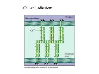
MEMS Cell Adhesion Device. Andrea Ho Mark Locascio Owen Loh Lapo Mori December 1, 2006. PDMS Membrane. PLA. Top Electrode. PVDF (Piezoelectric). Bottom Electrodes. PDMS. Via. SiO 2. Ni Traces (Layer 2). Parylene. Ni Traces (Layer 1). Si. Summary of Fabrication.

E N D
MEMS Cell Adhesion Device Andrea Ho Mark Locascio Owen Loh Lapo Mori December 1, 2006
PDMS Membrane PLA Top Electrode PVDF(Piezoelectric) Bottom Electrodes PDMS Via SiO2 Ni Traces (Layer 2) Parylene Ni Traces (Layer 1) Si Summary of Fabrication • Based on passive PDMS pillar arrays • Add 3-axis force sensitivity on each pillar • Thin membrane over pillars • Alignment is critical • Pillars, piezoelectric elements, electrodes • Use single set of alignment marks for all layers [Roure, et al. PNAS 2005]
Fabrication - Alignment Features • Si wafer • Deposit silicon nitride by LPCVD • Spincoat with resist • Pattern alignment features in resist • Etch silicon nitride using RIE • Strip resist in oxygen plasma
Fabrication - Pillar Mold • Spincoat with resist • Pattern resist by e-beam lithography • Etch Si using DRIE • Strip resist • (Silanize wafer to improve PLA release) • Pour PLA • Deposit common top electrode by e-beam evaporation
Fabrication - Piezoelectric Elements • Spincoat with PVDF (piezoelectric) • Spincoat with resist • Pattern using e-beam lithography • Etch PVDF using RIE • Strip resist
PVDF Electrodes Fabrication - Electrodes • Spincoat with PDMS • Pattern bottom electrodes and first set oftraces by e-beam lithography and liftoff • Deposit SiO2 dielectric layer by PECVD • Spincoat with e-beam resist and patternby e-beam lithography • Etch through SiO2 by RIE • Strip resist in acetone • Sputter with Ni • Spincoat with e-beam resist and patternby e-beam lithography • Etch exposed Ni • Strip resist • Deposit parylene by CVD
Fabrication - Wafer Bonding • Flip over and bond parylene layer to Si wafer with low heat and pressure • Peel off top Si wafer and SU-8 mold
PDMS Membrane • Begin with Si wafer • Spincoat with photoresist • Spincoat with diluted PDMS • (Treat in oxygen plasma)
Mold Release • Flip over PDMS-coated wafer and bond to pillars • Peel away support wafer • (Treat in oxygen plasma)
Parametric Study • Dependence of output voltage on • pillar geometry • Diameter • Height • Electrode geometry • material properties
FEM analysis Model geometry Mesh
FEM results It is reasonable to assume constant sz over the piezoelectric material.
Additional results Resonance frequency Tip displacement
Rwire CPVDF RPVDF Rwire Frequency Response • Lumped element model • Long, thin Ni wires in and out of pillar • Electrode of pillar modeled as parallel resistor & capacitor
Frequency Response • Circuit element values calculated from material properties
Zw Zw ZPR ZPC ZP ZEQ Zw Zw Frequency Response • Combine impedances • Take output across ZP
Frequency Response • Bode plot shows ωC >> any frequency we will be sensing
Thermal Noise • The electrodes and PVDF form an RC system • As in Senturia, this arrangement will create thermal noise in the system • Need to ensure RMS thermal noise << output voltages
Thermal Noise • Consider noisy resistor to be a noiseless resistor an a voltage source RPVDF VNOISE VOUT RPVDF CPVDF CPVDF
Thermal Noise • Calculate noise bandwidth • Calculate thermal noise • This is acceptable, since our outputs will be hundreds of mV
Actuation • Piezoelectrics allow for both actuation and sensing • Electromechanical coupling factor k • kPVDF≈ 0.1 to 0.3 • Easy to run in reverse to stimulate cell
Actuation • Applied voltages will have to be roughly 10x the voltage out for a corresponding deflection • This puts it at a reasonable value for actuation voltage • Actuation would have to be calibrated experimentally
Sensitivity Analysis • Change in voltage output for a given change in force: Slope of linear parametric plots
Sensitivity Analysis Resolution where system noise is the limiting factor
Sensitivity Analysis Resolution affected by fabrication processes • Effect of variation in pillar diameter on output voltage Diameter varies by ~10nm → Output voltage varies ~mV ΔV = (30mV/μm)(0.06 μm) = 1.8 mV
Sensitivity Analysis • Effect of PVDF layer uniformity (4% ) • At F = 100nN, ΔV[mV] = 450Δx[μm] • This results in an output voltage range of 36 mV • ΔF = 36 mV/5.5061 = 6.54 nN
Sensitivity Analysis • Effect of variation in pillar height • DRIE allows pillar height to vary ~μm • At F = 100nN, output voltage can range over 20 mV • Worst case scenario: • At F=100nN, output voltage varies over a total range of 20 + 36 + 1.8 mV = 57.8 mV • ΔF = 10.50 nN (~10% error)