Download
1 / 53
540 likes | 645 Vues
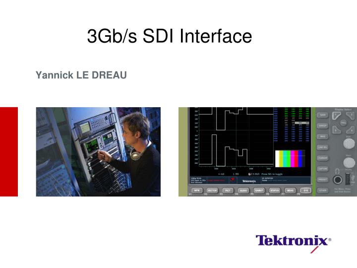
3Gb/s SDI Interface. Yannick LE DREAU. Agenda. SMPTE Standards for 3Gb/s Interface Physical Layer Specification Mapping Structures 3Gb/s Measurements 3Gb/s Test Signals. Hybrid Facility. Physical Layer. Transmission Media. Picture Formats. Sampling Structures.

E N D
3Gb/s SDI Interface Yannick LE DREAU
Agenda • SMPTE Standards for 3Gb/s Interface • Physical Layer Specification • Mapping Structures • 3Gb/s Measurements • 3Gb/s Test Signals 3Gb/s SDI Interface
Hybrid Facility Physical Layer Transmission Media Picture Formats Sampling Structures 3Gb/s SMPTE 424M 2048x1080 12-bit Dual Link SMPTE 372M 4:4:4:4 Blu-Ray 1.5Gb/s SMPTE 292M HD 1920x1080 RGB(A) RGB 1280x720 YCbCr SD 270Mb/s 4:2:2 720x480 Physical Layer Cable Type Termination Inter-Connections 10-bit 720x576 DVD 3Gb/s SDI Interface
Dual Link Format • Using existing HD-SDI infrastructure • Requires two signal paths • Link A & Link B • SMPTE 352M to identify links • Mapping various formats into existing HD-SDI structure • Problems • Interconnection issues • Swapped or Missing links • Cable Path different for each Link 3Gb/s SDI Interface
Why 3Gb/s SDI and High Speed Data? • Work at the highest resolution (Bit Depth and Colorspace) possible prior to rendering the product. • In standard HD-SDI limited to 4:2:2 YCbCr only at 10-bit • With Dual Link & 3Gb/s, users can: • Increase color range from 10 bits to 12 bits • Switch from 4:2:2 to 4:4:4 Sampling to the total chrominance Bandwidth • Work in the RGB domain for easier integration with Special Effects editors, and Telecine applications • Digital cinema cameras now being adopted for feature films, television shows, and even commercials • Panavision Genesis™ • Attack of the Clones, Revenge of the Sith, Apocalypto, … • Thomson Viper FilmStream™ 3Gb/s SDI Interface
Digital Active Line Active Picture or Ancillary Data Digital Active Line Active Picture or Ancillary Data Digital Line Blanking Blanking Level or Ancillary Data Digital Line Blanking Blanking Level or Ancillary Data SAV SAV SAV SAV EAV + Line No. + CRC EAV + Line No. + CRC SMPTE424M Signal/Data Serial Interface • Defines the transport of bit-serial data structure for 3.0Gb/s • Using a single coaxial cable interface • Supports either 10 or 12 bits data words • Mapped into two virtual interfaces • 10 bit parallel data streams (Data Stream One & Data Stream Two) Digital Line Period Data stream one of the virtual interface Interface Frequency 148.5MHz or 148.5/1.001 MHz Data stream two of the virtual interface Interface Frequency 148.5MHz or 148.5/1.001 MHz 3Gb/s SDI Interface
Digital Line Period Optional Ancillary Data Digital Active Line SAV(3FFh) SAV(000h) SAV(000h) SAV(XYZh) Y’ 0 Y’1 Y’2 Y’3 Y’1918 Y’1919 SAV(3FFh) SAV(3FFh) SAV(000h) SAV(000h) SAV(000h) SAV(000h) SAV(XYZh) SAV(XYZh) EAV(3FFh) EAV(3FFh) LN0 LN0 EAV(000h) LN1 LN1 EAV(000h) CR0 EAV(000h) EAV(000h) CR0 EAV(XYZh) CR1 EAV(XYZh) CR1 Image Structure • Example of image mapping structure for 4:2:2 YCbCr 10 bits 60/59.94 EAV + Line No. + CRC Digital Active Line Active Picture or Ancillary Data Digital Line Blanking SAV SAV Data Stream One Virtual Interface Optional Ancillary Data Digital Active Line Data Stream Two Virtual Interface SAV(3FFh) SAV(000h) SAV(XYZh) C’B’0 SAV(000h) C’R’0 C’B’1 C’R’1 C’B’959 C’R’959 3Gb/s SDI Interface
Optional Ancillary Data Digital Active Line Data Stream One Virtual Interface Y’2 Y’3 SAV(3FFh) SAV(000h) SAV(000h) SAV(XYZh) Y’ 0 Y’1 Y’1918 Y’1919 Optional Ancillary Data Digital Active Line Data Stream Two Virtual Interface C’B’1 C’R’1 SAV(3FFh) SAV(000h) SAV(000h) SAV(XYZh) C’B’0 C’R’0 C’B’959 C’R’959 Optional Ancillary Data Digital Active Line SAV(3FFh) SAV(3FFh) SAV(000h) SAV(000h) SAV(000h) SAV(000h) SAV(XYZh) SAV(XYZh) C’B’0 Y’ 0 C’R’0 Y’1 C’B’1 Y’2 C’R’1 Y’3 EAV(3FFh) EAV(3FFh) EAV(000h) EAV(000h) EAV(000h) EAV(000h) EAV(XYZh) EAV(XYZh) LN0 LN0 LN1 LN10 CR0 CR0 CR1 CR1 SAV(3FFh) SAV(3FFh) SAV(000h) SAV(000h) SAV(000h) SAV(000h) SAV(XYZh) SAV(XYZh) C’B’959 Y’1918 C’R’959 Y’1919 SAV(3FFh) SAV(3FFh) SAV(000h) SAV(000h) SAV(000h) SAV(000h) SAV(XYZh) SAV(XYZh) EAV(3FFh) LN0 LN0 EAV(3FFh) EAV(000h) LN1 LN1 EAV(000h) EAV(000h) EAV(000h) CR0 CR0 CR1 EAV(XYZh) EAV(XYZh) CR1 Image Structure Multiplexed • Data Stream one and two of the virtual interfaced are multiplexed together producing twice the data rate • Channel Coding uses NRZI Multiplexed 10-bit Parallel interface 3Gb/s SDI Interface
EAV SAV Optional Ancillary Data EAV(3FFh) EAV(000h) EAV(000h) EAV(XYZh) EAV(XYZh) LN0 SAV(3FFh) SAV(3FFh) SAV(000h) SAV(000h) SAV(000h) SAV(XYZh) SAV(XYZh) Y’ 0 Y’2 Y’3 C’B’959 Y’1918 C’R’959 EAV(3FFh) EAV(000h) EAV(000h) LN0 LN1 LN10 CR0 CR0 CR1 CR1 SAV(000h) C’B’0 C’R’0 Y’1 C’B’1 C’R’1 Y’1919 Mapping 2x SMPTE 292 HD-SDI Level B • Mapping of two parallel 10 bit interfaces with same line and frame structure in conformance with SMPTE292. • Payload Identifier CRC LN 10-bit multiplex in accordance with SMPTE 292M Interface clock frequency 148.5MHz or 148.5MHz/1.001 MHz 3Gb/s SDI Interface
Mapping 2x SMPTE 292 HD-SDI Level B 3Gb/s SDI Interface
Optional Ancillary Data C’r 959 Y’1919 C’b 0 Y’ 0 C’r 1 Y’ 1 SAV(3FFh) SAV(3FFh) SAV(000h) SAV(000h) SAV(000h) SAV(000h) SAV(XYZh) SAV(XYZh) EAV(3FFh) LN0 EAV(3FFh) LN0 LN1 EAV(000h) LN1 EAV(000h) CR0 EAV(000h) EAV(000h) CR0 CR1 EAV(XYZh) CR1 EAV(XYZh) Level B “Fast Progressive” Dual Link SMPTE372M SMPTE 274M 4:2:2 YCbCr 10 bit 60,59,94 & 50 Interface sampling frequency = 148.5MHz or 148.5/1.001 MHz as defined in SMPTE 274M Y’ Data Y’ 2 Y’ 3 Y’ 1918 Y’ 1919 Y’ 0 Y’ 1 Y’ 1920 Y’ 1921 Y’ 1922 Y’ 1923 Y’ 1924 Y’ 1925 Y’ 1926 Y’ 1927 Y’ (N-5) Y’ (N-4) Y’ (N-3) Y’ (N-2) Y’ (N-1) Y’ (N) C’b 959 C’b 960 C’b 961 C’b 962 C’b 963 C’b (N-2) C’b (N-1) C’b (N) C’b 0 C’b 1 Interface sampling frequency = 74.25MHz or 74.25/1.001 MHz as defined in SMPTE 274M C’b Data C’r 959 C’r 960 C’r 961 C’r 962 C’r 963 C’r (N-2) C’r (N-1) C’r (N) C’r 0 C’r 1 Interface sampling frequency = 74.25MHz or 74.25/1.001 MHz as defined in SMPTE 274M C’r Data Optional Ancillary Data Data Stream One Of the virtual interface Link A Interface sampling frequency = 148.5MHz or 148.5/1.001 MHz C’b 959 C’b 0 Y’ 0 Y’ 1 Y’1918 C’r 959 Y’1919 C’r 0 Data Stream Two Of the virtual interface Link B Interface sampling frequency = 148.5MHz or 148.5/1.001 MHz Y’1918 C’b 959 3Gb/s SDI Interface
Dual Link SMPTE372MSMPTE 274M 4:2:2 YCbCr 10 bit 60,59,94 & 50 3Gb/s SDI Interface
SMPTE425M Signal/Data Serial Interface Source Image Format (Level A) 3Gb/s SDI Interface
Comparison of Level A vs. Level B • 1080p 50/59.94/60 • SMPTE 425 Mapping structure 1 – alternates Y and Cb/Cr samples, effect is similar to standard HD-SDI but at twice the rate • SMPTE 372M §4.1 – alternates entire lines, each with Y and Cb/Cr 3Gb/s SDI Interface
Optional Ancillary Data C’B’1 C’R’1 C’B’0 C’R’0 C’B’959 C’R’959 SAV(3FFh) SAV(3FFh) SAV(000h) SAV(000h) SAV(000h) SAV(000h) SAV(XYZh) SAV(XYZh) LN0 EAV(3FFh) EAV(3FFh) LN0 LN1 EAV(000h) LN1 EAV(000h) CR0 EAV(000h) EAV(000h) CR0 EAV(XYZh) CR1 CR1 EAV(XYZh) SMPTE 425M Mapping 1SMPTE 274M 4:2:2 YCbCr 10 bit 60,59,94 & 50 Interface sampling frequency = 148.5MHz or 148.5/1.001 MHz as defined in SMPTE 274M Y’ Data Y’2 Y’3 Y’1918 Y’1919 Y’ 0 Y’1 Y’1920 Y’1921 Y’1922 Y’1923 Y’1924 Y’1925 Y’1926 Y’1927 Y’ (N-5) Y’ (N-4) Y’ (N-3) Y’ (N-2) Y’ (N-1) Y’ (N) C’B959 C’B960 C’B961 C’B962 C’B963 C’B (N-2) C’B (N-1) C’B (N) C’B 0 C’B 1 Interface sampling frequency = 74.25MHz or 74.25/1.001 MHz as defined in SMPTE 274M C’b Data C’R959 C’R960 C’R961 C’R962 C’R963 C’R (N-2) C’R (N-1) C’R (N) C’R 0 C’R 1 Interface sampling frequency = 74.25MHz or 74.25/1.001 MHz as defined in SMPTE 274M C’r Data Optional Ancillary Data Interface sampling frequency = 148.5MHz or 148.5/1.001 MHz Data Stream One Of the virtual interface Y’2 Y’3 Y’ 0 Y’1 Y’1918 Y’1919 Interface sampling frequency = 148.5MHz or 148.5/1.001 MHz Data Stream Two Of the virtual interface 3Gb/s SDI Interface
SMPTE 425M Mapping 1 Data Display Data mode SMPTE 274M 4:2:2 YCbCr 10 bit 60,59,94 & 50 3Gb/s SDI Interface
SMPTE 425M Mapping 1 Data Display Video modeSMPTE 274M 4:2:2 YCbCr 10 bit 60,59,94 & 50 3Gb/s SDI Interface
Y0 G0 Pr0 R0 G1 Y1 R1 Pr1 G2 Y2 Pr2 R2 A0 A0 B0 Pb0 A1 A1 Pb1 B1 A2 A2 Pb2 B2 SMPTE 425M Mapping 24:4:4:4 RGB (A) or 4:4:4:4 YCbCr (A) 10-bit Data Stream One Data Stream Two 3Gb/s SDI Interface
R’(N-1) R’ 0 R’ 1 R’(N-2) B’(N-2) B’(N-1) R’ (N) B’ (N) B’ 0 B’ 1 B’(a) B’(a+2) A (a) A (a+1) B’(a+1) A (a+2) A (a+3) B’(a+3) A (a+4) B’(a+4) R’(a) R’(a+2) R’(a+1) R’(a+3) R’(a+4) A (N-2) A (N) A (N-1) A 0 A 1 SAV(3FFh) SAV(3FFh) SAV(000h) SAV(000h) SAV(000h) SAV(000h) SAV(XYZh) SAV(XYZh) EAV(3FFh) LN0 EAV(3FFh) LN0 EAV(000h) LN1 LN1 EAV(000h) EAV(000h) CR0 EAV(000h) CR0 EAV(XYZh) CR1 CR1 EAV(XYZh) SMPTE 425M Mapping 24:4:4:4 RGB (A) or 4:4:4:4 YCbCr (A) 10-bit G’(N-1) G’ 0 G’ 1 G’(N-2) G’ (N) G’(a-1) G’(a) G’(a+2) G’(a+1) G’(a+3) G’(a+4) Interface sampling frequency = 74.25MHz or 74.25/1.001 MHz as defined in SMPTE 274M G’ / Y’ Data B’(a-1) Interface sampling frequency = 74.25MHz or 74.25/1.001 MHz as defined in SMPTE 274M B’ / C’b Data R’(a-1) Interface sampling frequency = 74.25MHz or 74.25/1.001 MHz as defined in SMPTE 274M R’/ C’b Data A (a-1) Interface sampling frequency = 74.25MHz or 74.25/1.001 MHz as defined in SMPTE 274M A’ Data Optional Ancillary Data Interface sampling frequency = 148.5MHz or 148.5/1.001 MHz Data Stream One Of the virtual interface G’1 R’1 G’(a-1) R’(a-1) G’ (a) R’ (a) G’ 0 R’0 Optional Ancillary Data Interface sampling frequency = 148.5MHz or 148.5/1.001 MHz Data Stream Two Of the virtual interface A (a-1) B’ (a-1) A (a) B’ (a) A 1 B’1 A 0 B’0 3Gb/s SDI Interface
Comparison of Level A vs. Level B • 4:4:4(:4) 10-bit • SMPTE 425 Mapping structure 2 – R samples always on stream 1, B on stream 2. Alpha channel on stream 2. • SMPTE 372M §4.2 – Even B+R samples on stream 1, odd B+R samples on stream 2. Alpha channel on stream 2. 3Gb/s SDI Interface
RGB/XYZ[11:9] a/n RGB/XYZ[5:3] a/n RGB/XYZ[11:9 ] a+1/n+1 RGB/XYZ[5:3] a+1/n+1 RGB/XYZ[11:9 ] a+2/n+2 RGB/XYZ[5:3] a+2/n+2 RGB/XYZ[8:6] a/n RGB/XYZ[2:0] a/n RGB/XYZ[8:6] a+1/n+1 RGB/XYZ[2:0] a+1/n+1 RGB/XYZ[8:6 ] a+2/n+2 RGB/XYZ[2:0] a+2/n+2 SMPTE 425M Mapping 34:4:4 RGB or 4:4:4 YCbCr or XYZ 12-bit Data Stream One Data Stream Two G’B’R’/X’Y’Z’(a) / (n) [x:y] bit structure mapping into data words of the virtual interface 3Gb/s SDI Interface
GBR/XYZ[11:9] a/n GBR/XYZ[5:3] a/n GBR/XYZ[11:9 ] a+1/n+1 GBR/XYZ[5:3] a+1/n+1 GBR/XYZ[11:9 ] a+2/n+2 GBR/XYZ[5:3] a+2/n+2 GBR/XYZ[8:6] a/n GBR/XYZ[2:0] a/n GBR/XYZ[8:6] a+1/n+1 GBR/XYZ[2:0] a+1/n+1 GBR/XYZ[8:6 ] a+2/n+2 GBR/XYZ[2:0] a+2/n+2 SMPTE 425M Mapping 34:4:4 RGB or 4:4:4 YCbCr or XYZ 12-bit Data Stream One Data Stream Two Location of the first and last active samples for 4:4:4 (R’G’B’) and (X’Y’Z’)/12-bit Signals 3Gb/s SDI Interface
C'B(N-1) C'R (N-1) C'B 0 C'R 0 C'B 1 C'R 1 C'B(N-2) C'R (N-2) C'B (N) C'R (N) C'B (a+1) C'R (a+1) C'R (a+3) C'B (a+3) C'R (a+4) C'B (a+4) C'B (a) C'R (a) C'B (a+2) C'R (a+2) SAV(3FFh) SAV(3FFh) SAV(000h) SAV(000h) SAV(000h) SAV(000h) SAV(XYZh) SAV(XYZh) LN0 EAV(3FFh) EAV(3FFh) LN0 EAV(000h) EAV(000h) LN1 LN1 CR0 EAV(000h) EAV(000h) CR0 CR1 EAV(XYZh) EAV(XYZh) CR1 SMPTE 425M Mapping 34:4:4 RGB or 4:4:4 YCbCr or XYZ 12-bit GBR/XYZ[11:9] a/n GBR/XYZ[5:3] a/n GBR/XYZ[11:9 ] a+1/n+1 GBR/XYZ[5:3] a+1/n+1 GBR/XYZ[11:9 ] a+2/n+2 GBR/XYZ[5:3] a+2/n+2 Data Stream One GBR/XYZ[8:6] a/n GBR/XYZ[2:0 ] a/n GBR/XYZ[8:6] a+1/n+1 GBR/XYZ[2:0] a+1/n+1 GBR/XYZ[8:6 ] a+2/n+2 GBR/XYZ[2:0] a+2/n+2 Data Stream Two G/X (N-1) G/X 0 G/X 1 G/X (N-2) G/X (N) G/X (a+1) G/X (a+3) G/X (a+4) G/X (a-1) G/X (a) G/X (a+2) Interface sampling frequency = 74.25MHz or 74.25/1.001 MHz as defined in SMPTE 274M G’/ Y’ /X’ Data C'B (a-1) Interface sampling frequency = 74.25MHz or 74.25/1.001 MHz as defined in SMPTE 274M B’/ C’b /Y’ Data C'R (a-1) Interface sampling frequency = 74.25MHz or 74.25/1.001 MHz as defined in SMPTE 274M R’/ C’r /Z’ Data Optional Ancillary Data Interface sampling frequency = 148.5MHz or 148.5/1.001 MHz Data Stream One Of the virtual interface RGB(1)11:9 RGB(1)5:3 RGB(0)11:9 RGB(0)5:3 RGB(a-1)11:9 RGB(a-1)5:3 RGB (a)11:9 RGB (a)5:3 Optional Ancillary Data Interface sampling frequency = 148.5MHz or 148.5/1.001 MHz Data Stream Two Of the virtual interface RGB (1)8:6 RGB (1)2:0 RGB (0)8:6 RGB (0)2:0 RGB (a-1)8:6 RGB (a-1)2:0 RGB (a)8:6 RGB (a)2:0 3Gb/s SDI Interface
C'B(N-1) C'R (N-1) C'B 0 C'R 0 C'B 1 C'R 1 C'B(N-2) C'R (N-2) C'B (N) C'R (N) C'B (a+1) C'R (a+1) C'R (a+3) C'B (a+3) C'R (a+4) C'B (a+4) C'B (a) C'R (a) C'B (a+2) C'R (a+2) SAV(3FFh) SAV(3FFh) SAV(000h) SAV(000h) SAV(000h) SAV(000h) SAV(XYZh) SAV(XYZh) LN0 EAV(3FFh) EAV(3FFh) LN0 EAV(000h) EAV(000h) LN1 LN1 CR0 EAV(000h) EAV(000h) CR0 CR1 EAV(XYZh) EAV(XYZh) CR1 SMPTE 425M Mapping 34:4:4 XYZ 12-bit GBR/XYZ[11:9] a/n GBR/XYZ[5:3] a/n GBR/XYZ[11:9 ] a+1/n+1 GBR/XYZ[5:3] a+1/n+1 GBR/XYZ[11:9 ] a+2/n+2 GBR/XYZ[5:3] a+2/n+2 Data Stream One GBR/XYZ[8:6] a/n GBR/XYZ[2:0 ] a/n GBR/XYZ[8:6] a+1/n+1 GBR/XYZ[2:0] a+1/n+1 GBR/XYZ[8:6 ] a+2/n+2 GBR/XYZ[2:0] a+2/n+2 Data Stream Two G/X (N-1) G/X 0 G/X 1 G/X (N-2) G/X (N) G/X (a+1) G/X (a+3) G/X (a+4) G/X (a-1) G/X (a) G/X (a+2) Interface sampling frequency = 74.25MHz or 74.25/1.001 MHz as defined in SMPTE 274M G’/X’ Data C'B (a-1) Interface sampling frequency = 74.25MHz or 74.25/1.001 MHz as defined in SMPTE 274M B’/Y’ Data C'R (a-1) Interface sampling frequency = 74.25MHz or 74.25/1.001 MHz as defined in SMPTE 274M R’/Z’ Data Optional Ancillary Data Interface sampling frequency = 148.5MHz or 148.5/1.001 MHz Data Stream One Of the virtual interface XYZ(1)11:9 XYZ(1)5:3 XYZ(0)11:9 XYZ(0)5:3 XYZ(a-1)11:9 XYZ(a-1)5:3 XYZ(a)11:9 XYZ(a)5:3 Optional Ancillary Data Interface sampling frequency = 148.5MHz or 148.5/1.001 MHz Data Stream Two Of the virtual interface XYZ (1)8:6 XYZ (1)2:0 XYZ (0)8:6 XYZ (0)2:0 XYZ (a-1)8:6 XYZ (a-1)2:0 XYZ (a)8:6 XYZ (a)2:0 3Gb/s SDI Interface
Comparison of Level A vs. Level B 4:4:4 12-bit SMPTE 425 Mapping structure 3 – every 10 bit word includes 3 bits of each of the three channels (four words comprise complete sample) SMPTE 372M §4.3 and §4.4 – most significant 10 bits of the three channels appear as in §4.2 formats, and two LSBs of each channel are grouped together into a single word that displaces the A channel
Y[11:6] a-1/n-1 Y[5:0] a-1/n-1 Y[11:6 ] a/n Y[5:0] a/n Y[11:6 ] a+1/n+1 Y[5:0] a+1/n+1 Cb[11:6] a/n Cb[5:0 ] a/n Cr[11:6] a/n Cr[5:0] a/n Cb[11:6 ] a+1/n+! Cb[5:0] a+1/n+1 SMPTE 425M Mapping 44:2:2 YCbCr 12 bit • G’/X’ samples maybe replaced with Y’ samples • B’/Y’ samples maybe replaced with C’b samples • R’/Z’ samples maybe replaced with C’r samples Data Stream One Data Stream Two 3Gb/s SDI Interface
SMPTE 425M Mapping 44:2:2 YCbCr 12 bit Y[11:6] a-1/n-1 Y[5:0] a-1/n-1 Y[11:6 ] a/n Y[5:0] a/n Data Stream One Data Stream Two Cb[11:6] a/n Cb[5:0 ] a/n Cr[11:6] a/n Cr[5:0] a/n 3Gb/s SDI Interface
SAV(3FFh) SAV(3FFh) SAV(000h) SAV(000h) SAV(000h) SAV(000h) SAV(XYZh) SAV(XYZh) EAV(3FFh) LN0 EAV(3FFh) LN0 EAV(000h) EAV(000h) LN1 LN1 EAV(000h) EAV(000h) CR0 CR0 CR1 EAV(XYZh) EAV(XYZh) CR1 SMPTE 425M Mapping 44:2:2 YCbCr 12 bit Y[11:6] a-1/n Y[5:0] a-1/n Y[11:6 ] a/n Y[5:0] a/n Data Stream One Data Stream Two Cb[11:6] a/n Cb[5:0 ] a/n Cr[11:6] a/n Cr[5:0] a/n Interface sampling frequency = 74.25MHz or 74.25/1.001 MHz as defined in SMPTE 274M Y’ Data Y’2 Y’3 Y’ 0 Y’1 Y’(a-3) Y’(a-2) Y’(a-1) Y’(a+1) Y’(a+2) Y’ (a+3) Y’ (a+4) Y’ (N-3) Y’ (N-2) Y’ (N-1) Y’ (N) Y’ (a) C'B(N-1) C'B 0 C'B 1 C'B (N) C'B (a+1) C'B (a-1) C'B (a) C'B (a+2) Interface sampling frequency = 37.125MHz or 37.125/1.001 MHz as defined in SMPTE 274M C’B Data C'R (N-1) C'R 0 C'R 1 C'R (N) C'R (a-1) C'R (a+1) C'R (a) C'R (a+2) Interface sampling frequency = 37.125MHz or 37.125/1.001 MHz as defined in SMPTE 274M C’R Data Optional Ancillary Data Interface sampling frequency = 148.5MHz or 148.5/1.001 MHz Data Stream One Of the virtual interface Y’ (1)11:6 Y’ -1)5:0 Y’ (0)11:6 Y‘ (0)5:0 Y’ (a-1)11:6 Y’ (a-1)5:0 Y’ (a)11:6 Y’ (a)5:0 Optional Ancillary Data Interface sampling frequency = 148.5MHz or 148.5/1.001 MHz Data Stream Two Of the virtual interface C’R (0)11:6 C’R (0)5:0 C’B (0)11:6 C’B (0)5:0 C’B (a)11:6 C’B (a)5:0 C’R (a)11:6 C’R (a)5:0 3Gb/s SDI Interface
Comparison of Level A vs. Level B 4:2:2 12-bit SMPTE 425 Mapping structure 4 – two 10 bit words each carry 6 bits of each of the three channels. No alpha channel is supported, despite the available space (four bits unused per word). SMPTE 372M §4.5 – Stream 1 carries the 10 MSBs of each sample in the familiar Cb/Y/Cr/Y sequence, and stream 2 carries a word of LSBs (2 bits per channel) plus a 10 bit alpha channel.
3Gb/s Serial Digital Interface • Pk-to-Pk Amplitude 800mV +/- 10% • DC Offset 0.0V +/- 0.5V • Rise/Fall Time between 20% & 80% no greater than 135ps and not differ by more than 50ps • Overshoot rise/fall not to exceed 10% of amplitude • Timing Jitter <= 2UI above 10Hz • Alignment Jitter <= 0.3UI above 100kHz 3Gb/s SDI Interface
Eye Specifications per SMPTE Standards 3Gb/s SDI Interface
How to Make Eye Measurement • Eye Display • Launch Amplitude • Short Length of Cable • Color Bar Test Signal • Automated Measurements • Available on WM8300 • Amplitude Histogram • Simplifies The Task • Infinite persistence can aid in seeing eye opening 80% Rise Time Fall Time Amplitude 20% 3Gb/s SDI Interface
Eye Pattern Distortions • Long cable • Decrease in amplitude • Decrease in Frequency response • Eye opening narrows • Rise/Fall time increases • Termination • Incorrect termination causes overshoot and undershoot • Shift in Eye Crossing • Shifts 50% point of eye opening • Caused by unequal rise or fall time 3Gb/s SDI Interface
Jitter Measurements • Timing Jitter • Alignment Jitter The variation in position of a signal’s transitions occurring at a rate greater than a specified frequency, typically 10Hz The variation in position of a signal’s transitions relative to those of a clock extracted from the signal. 3Gb/s SDI Interface
What is Jitter? • Definition: Jitter is defined as the variation of a digital signal’s significant instants (such as transition points) from their ideal positions in time. • Time Interval Error – Jitter • Introduced by frequency, amplitude and phase variation in signals transition 3Gb/s SDI & Advanced Data Analysis
Types of Jitter • Types of Jitter • Random • Random Process • No Discernible pattern • All devices have random jitter present • Thermal or shot noise • Model by Gaussian distribution • Deterministic • Switching PSU • Frequency response • cable or device • Rise/Fall Time of Transition 3Gb/s SDI & Advanced Data Analysis
Why noise can introduce jitter 3Gb/s SDI & Advanced Data Analysis
Cable frequency responce introduces jitter • Risign edges have high frequency content • Repetitive patterns have lower frequency content • Frfequencies travel at different speed in the cable (group delay) • This effect is visible only with long cables 3Gb/s SDI & Advanced Data Analysis
Methods of Measuring Jitter • The Equivalent-time Eye method constructs an • Equivalent-time Eye diagram of the signal and measures the amount the edge samples in the Eye vary from their ideal positions. • The Real-time Acquisition method • Applies signal processing algorithms to one or more acquisition records captured in real-time from single trigger events to measure the amount each signal edge in the acquisition record varies from its ideal position. • The Phase Demodulation method • Applies two appropriately filtered clock signals to a phase detector. The output from the phase detector is the demodulated jitter signal. • Color Bar Test signal Recommended not Pathological 3Gb/s SDI & Advanced Data Analysis
EQ time Acquisition 3Gb/s SDI & Advanced Data Analysis
Phase demodulation Method 3Gb/s SDI & Advanced Data Analysis
PK-Pk but in which time interval? 3Gb/s SDI & Advanced Data Analysis
How to Make Jitter Measurements • Jitter Meter shows direct readout • Ability to measure Timing and Alignment jitter simultaneously • Jitter waveform show variation of signal related to line and field rate of video signal 3Gb/s SDI Interface
HD3G73 Gb/s SDI Generator/Converter Module for the TG700 • All 1080-line formats of SMPTE 425 now supported • YPbPr 4:2:2/4:4:4 10/12-bit • RGB 4:4:4 10/12-bit • XYZ 4:4:4 12-bit • Complete coverage of both Level A and Level B mappings • Wide variety of standard test signals • Two signal outputs • HD-SDI input for up-converter function • Trigger output (frame pulse or 148.5 MHz clock) for external oscilloscope synchronization 3Gb/s SDI Interface
SDI Checkfield Test Pattern • Defined in SMPTE RP 198 for HD-SDI • Equalizer test pattern has maximum DC content • Uses 20 bit pattern 1100000000 0110011000 (300h 198h) input to the scrambler for the serial data stream • Produces output with repeated pattern of 19 consecutive high (low) states followed by 1 low (high) state • Corresponds to Y=198h, Cb=Cr=300h (shade of magenta) for HD-SDI 3Gb/s SDI Interface
SDI Checkfield Test Pattern • PLL test pattern has maximum low-frequency content and minimum high-frequency content • Uses 20 bit pattern 1000000000 0100010000 (200h 110h) input to the scrambler for the serial data stream • Produces output with repeated pattern of 20 consecutive high (low) states followed by 20 consecutive low (high) state • Corresponds to Y=110h, Cb=Cr=200h (23.74% gray) for HD-SDI 3Gb/s SDI Interface
SDI Checkfield Test Pattern for 3G-SDI • Why are the colors wrong? • In order to produce the same pathological patterns in the serial bit stream, the 10 bit words must be sequenced in the same order • This results in different colors from the familiar magenta/gray for various 3G mapping structures Data stream 1 carries the Y samples and data stream 2 carries the Cb/Cr samples, so the multiplexing is similar to HD-SDI and the pattern has the familiar colors. In dual link, lines alternate between the two links. Therefore, in Level B, odd lines have one word for both Y and Cb/Cr samples, and even lines have the other word for both Y and Cb/Cr samples. Level A MS1 (1080p) Level B 1080p 3Gb/s SDI Interface
SDI Checkfield Test Pattern for 3G-SDI • As it appears for other Level B formats: • Verify with data mode (not video mode) of data display 4:4:4 YCbCr 10-bit 4:4:4 GBR 12-bit 4:2:2:4 YCbCrA 12-bit 3Gb/s SDI Interface