Download
1 / 26
260 likes | 369 Vues
Automated TFT Noise Characterization Platform. Kendell Clark (EE), Stephen Marshall (EE), Carmen Parisi (EE), James Spoth (CE), Ryan Vaughan (ME) Rochester Institute of Technology Analog Devices Integrated Microsystems Laboratory. Agenda. Project Overview Customer Needs Specifications

E N D
Automated TFT Noise Characterization Platform Kendell Clark (EE), Stephen Marshall (EE), Carmen Parisi (EE), James Spoth (CE), Ryan Vaughan (ME) Rochester Institute of Technology Analog Devices Integrated Microsystems Laboratory
Agenda • Project Overview • Customer Needs • Specifications • Functionality so far • System Design • Schedule • Budget • Current Status
Project Overview • Noise Measurements of Thin-Film Devices on Glass is necessary for understanding their operation and modeling their behavior • Many noise measurements are required to accurately model any new technology • 1/f Noise measurements take a long time due to extremely low frequencies (1 mHz) • Devices under test must be accurately biased for the entire duration
Project Overview • Design & build an automated low noise measurement environment • Computer-Controlled Low noise biasing • Low noise signal amplification • Interface with and unify operation of laboratory measurement apparatus • Lower budget than competing commercial solutions • Cascade Microtech EDGE 1/f Noise Management System: • $1.2 million, but has more functionality • Thermal Chuck, Automated Probers, Automated Data Analysis, Higher Bandwidth, etc. • Aimed at commercial foundries improving process for marketing high-performance silicon • ADIML VIKING Platform • Approximately $1,000 • “Bare bones” automated noise measurements • Aimed at low budget research groups for characterization, rather than production testing
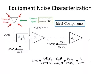
Customer Needs • EMI/RFI Shielded Environment • Localized, low noise amplification of DUT noise signal • Low noise, programmable DC biasing of DUT • Immunity from 60Hz AC power interference • Full noise measurement cycle is software-controllable • IV Sweep Device Bias Noise Measurement Data Acquisition • Interface with existing wafer probe station • Maintain full movement of wafer chuck and microscope gantry • Maintain view of wafer during measurement; RF shielding must remain • System must operate for several hours at a time • No clocks or oscillators inside shielded environment
Specifications - Problems • Issue with current bias circuit prevents circuit from settling. • Recent simulations show this can be fixed easily • Drain bias current resolution not yet measurable: • Nano- or pico-ammeter not available, still developing a measurement circuit using LNA to amplify current • LNA has an offset voltage that affects results at high gain settings • Battery life untested. • 9V batteries purchased could not output enough current for the circuit • Need to purchase new batteries
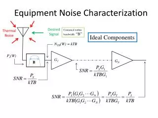
Analog Circuitry – Voltage Bias Circuitry • Control Voltage comes from a DAC located on the PCB. • RFilter & C form a LPF with corner frequency of 1mHz. • >60dB attenuation of noise in the measurement frequency range, 1Hz to 100kHz • RCharge allows for capacitor to reach desired voltage levels quickly.
Resistor-Based Current Bias Generation • Uses battery and resistor, or op-amp biasing scheme to produce a fixed voltage across a resistor • Fundamentally limited in noise performance • Resistor thermal noise floor of RD Image: Kwok K. Hung, et. Al. A Physics Based MOSFET Noise Model for Circuit Simulators. IEEE Trans. On Electron Devices. Vol. 37. May 1990.
Analog Circuitry – Current Bias Circuitry • Uses a JFET-based current source • Permits isolation of resistors from output current • Allows resistors to be filtered without attenuating noise at higher frequencies • Circuit topology offers output impedance enhanced by amplifier gain
Analog Circuitry – Current Bias Circuitry Equivalent Noise Model • Use superposition to find contribution of each noise source to output noise current • Choose Cs to attenuate all noise sources appropriately • Assuming large Cs, in1, vn1, inr are made negligible • Amplifier with low vn2 was chosen • JFETs have naturally low in,ch System achieves total output noise current on the order of 100 pA/√Hz
Analog Circuitry – LNA Noise Contribution Noise Analysis of LNA dictates that an amp with a low input voltage noise is chosen Total noise contribution found to be 25 pV/√Hz with AD797 amp
Digital Hardware • Xilinx Coolrunner II CPLD • No internal oscillators • Flexible I/O (Voltage levels, current drive, 33 I/O pins) • Low Cost (< $3) • Familiarity with design environment • Chose Peripherals with Serial Interface • Kept CPLD resource usage low (risk of running out of logic) • Allowed communication protocols to be implemented in software • AD5754BREZ DAC • Maxim MAX1248 ADC • On-Semi AMIS 39101 Relay Drivers • Used a CPLD register for power control lines
Control Software • Developed using LabVIEW • Initial effort at learning the language difficult • Reaping the benefits now (easy maintenance) • Developed highly modular code • Large hierarchy of Virtual Instruments makes high-level modifications easy • Implements peripheral-specific protocols in LabVIEW code • Should make adding additional functionality easier than modifying CPLD hardware or microcontroller firmware • Each register, whether located in the CPLD or a peripheral has a VI which makes setting parameters easy (top level module performs no protocol or bit setting operations) • Easy interface with Dynamic Signal Analyzer and 6501 USB DAQ
Hardware/Software Testing • Initial testing performed without any hardware • Oscilloscope to verify software • Simulations to verify CPLD design • Once PCB arrived and was assembled hardware testing began • Experienced typical hiccups • Verified functionality of CPLD communication and control of power bits • Only design error was an incorrect pinout of JTAG header • Fixed using Xilinx flying leads connector
Schedule • PCB build was delayed several weeks due to several issues: • Soldering was extra work due to lack of solder mask and high component density • Circuit bugs due to schematic entry error (ExpressPCB has no simulator) • Circuit bugs due to design errors • PCB reworks • Full functional/specification testing delayed due to circuit board bugs • Mechanical design delayed due to extracurricular circumstances • On track to be finished very soon
Budget • EMI Enclosure Materials • Metal: $150 • RF Glass and Gasket: $30 • JB Weld: $5 • NI6501A USB DAQ: $100 • Electrical Components: $340 • PC Board: $60, +$100 for final version • Batteries and Charging Solution: $70 • Total: $855 • Not accounted for: • NI LabView License • Xilinx CPLD Programming Cable: $295 • Probe Card: $500 ~ $1000, depending on application
Current Status • Mechanical design fits on probe station and meets all specifications • Scheduled for completion • Still finding bugs in the circuit • Pin-compatible, rail-to-rail amps are available • If that allows the circuit to work, the final PCB can be ordered • Simulations indicate that this was the problem
Digital Hardware / Software Status • CPLD modifications for new relay drivers complete • Including Simulations • Control Software needs updating for new relay drivers • Was pending completion of PCB v2 layout • Need to perform hardware validation of DAC control • DAC has never been soldered to board • Oscilloscope measurements at the right CPLD pins looked correct
References • [1] Johns, David A. and Ken Martin. Analog Integrated Circuit Design. John Wiley and Sons. 1997. • [2] Stanford Research Systems. Model SR570 – Low Noise Current Preamplifer. SRS, Inc. 1997. • [3] Kwok K. Hung, et. Al. A Physics Based MOSFET Noise Model for Circuit Simulators. IEEE Trans. On Electron Devices. Vol. 37. May 1990.
Acknowledgements • Dr. Robert J. Bowman, Faculty Advisor and Principal Investigator • Professor George Slack, Faculty Mentor and Guide