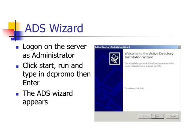
Download
1 / 26
260 likes | 524 Vues
Xilinx: new module. Architecture Wizard and PACE. FPGA Design Flow Workshop. Objectives. After completing this module, you will be able to: List two uses for the Architecture Wizard Identify two features in PACE. Outline. Architecture Wizard PACE Summary. Architecture Wizard.

E N D
Xilinx: new module Architecture Wizard and PACE FPGA Design Flow Workshop
Objectives After completing this module, you will be able to: • List two uses for the Architecture Wizard • Identify two features in PACE
Outline • Architecture Wizard • PACE • Summary
Architecture Wizard • Architecture Wizard contains two wizards: • Clocking Wizard • RocketIO Wizard • Double-click Create New Source • Select IP (CoreGen & Architecture Wizard), then click Next • Expand Clocking and select desired function • Expand I/O Interfacesand select RocketIO*
Clocking Wizard • Main window • Select pins • Specify… • Reference source • Clock frequency • Phase shift • Advanced button • Adding buffers • Connect clock buffers (BUFG, BUFGMUX) to selected output pins of the DCM
Clocking Wizard • Frequency synthesizer • Select M / D value OR • Specify frequency • “Calculate” button for jitter • Period jitter is evaluated for CLKFX output Note: This dialog appears only if the CLKFX output was selected
RocketIO Wizard • SelectIO™ standard • Transmitter • Pre-emphasis, voltage swing, CRC • Receiver • Comma detection 10B/8B selection • Clock correction, elastic buffer, bonding • Byte width specification • Termination impedance Pictured on the right is one of several dialogs
Attributes • By default, attributes are written into the HDL files • Example: Verilog with Synplicity • Simulation attributes are passed through ‘defparam • defparam DCM_INST.CLKDV_DIVIDE=2; • Synthesis attributes are passed within metacomments • /*synthesis xc_props=“CLK_FEEDBACK=1x, CLKDV_DIVIDE=2, …..*/;” • Alternatively, the UCF flow can be used to customize the components • The Wizard can also generate a file suffixed “_arwz.ucf” • Just cut and paste from “_arwz.ucf” file to the main UCF file • Remove attributes from the generated HDL file
Outline • Architecture Wizard • PACE • Summary
What is PACE? • Pinout and Area Constraints Editor • Pin Assignment • Assign I/O locations, specify I/O banks and I/O standards, prohibit I/O locations • Verify pin type to logic assignment • Perform DRC check to prevent illegal placements • Area Constraints • Create area constraints for logic and display I/Os on the periphery to show connectivity • Begin floorplanning early in the design flow • Verify area constraints
Using PACE • Assign pins and create area constraints for an existing design • After creating HDL code, launch PACE • Assign pin locations and area constraints • Select File Save to save UCF file • Plan your pinout and create a skeleton top-level HDL file for a new design • In PACE, select File New and choose Create New UCF and Design • Enter file names for new UCF and new top-level HDL file (VHDL or Verilog) • Enter pin names and locations in PACE GUI • Select File Save to save UCF and HDL files
Synthesized Netlist Design Flow with PACE (Post-Synthesis) • Reads synthesized netlist • Creates or modifies UCF file Design Source PACE Translate design.ucf design.lfp Complete Implementation
Synthesized Netlist Design Flow with PACE (Post-Translate) • Reads NGD file from Translate • Creates or modifies UCF file Design Source design.ucf Translate design.ncf design.ngd PACE design.ucf design.lfp Translate Complete Implementation
design.v/.vhd design.lfp Design Flow with PACE (New Design) • Creates top-level HDL file • Contains port information only • Use this file as a starting point for writing remaining HDL code • Creates UCF file for implementation PACE design.ucf Write HDL code & Synthesize NGDBuild Complete Implementation
PACE GUI • Design Hierarchy window • Displays different types of design elements • Design Object List window • Lists design elements based on the selected folder in the Design Hierarchy window • Use this window to create groups of I/O signals • Assign I/O signals or groups to specific pins, banks, or die edges • Enter I/O standards
PACE GUI • Device Architecture window • Displays banks and differential pairs • Define and display area constraints here • Package Pin window • Shows I/O banks • Displays differential pairs • Easy to assign pin locations • Table entry or drag-and-drop
Locking Pins • In the Design Hierarchy window, select I/O Pins • Make pin assignments in the Design Object List window • Type pin locations in the Location column • Select an I/O bank instead of assigning specific pins • Drag-and-drop pins into the Device Architecture or Package Pin windows
I/O Layout • I/O for control signals on the top or bottom • Signals are routed vertically • I/O for data buses on the left or right • FPGA architecture favors horizontal data flow General guidelines: Control Signals Data Flow Data Buses Data Buses Control Signals
Data Bus Layout • Arithmetic functions with more than five bits typically utilize carry logic • Carry chains require specific vertical orientation MSB LSB
Other PACE Features • Tools menu • Run Design Rule Check (DRC): Checks that all pins assigned to each bank use compatible I/O standards • SSO Analysis: Flags potential ground bounce problems caused by pin assignments • Clock Analysis: Displays clock distribution to each quadrant of the device • Package migration: When a design has the possibility of moving to a different device or package, PACE can display incompatible pins to help with pinout planning • IOB Make Pin Compatible With
Pin Compatibility Modified Package View after Pin compatibility is applied with 2V40-FG256 Original Package View of 2V250-FG256
Outline • Architecture Wizard • PACE • Summary
Review Questions • What are the advantages of using the Architecture Wizard in your design? • What are at least two features available in PACE?
Answers • What are the advantages of using the Architecture Wizard in your design? • You are not required to create the instantiation on your own • Automatically creates usable source code • Synthesis and simulation attributes are already written • Easy-to-use dialog boxes • What are at least two features available in PACE? • Drag-and-drop I/Os and area locations onto device package and layout windows • DRC checking • Ability to enter I/O standards • Prohibit and Allow sites • Easy package migration
Summary • The Architecture Wizard consists of two parts: • Clocking Wizard • RocketIO Wizard • PACE allows you to assign I/O locations easily and create area constraints for logic
Where Can I Learn More? • Architecture Wizard • “More Info” buttons in dialog boxes • PACE Online Help