Download
1 / 35
350 likes | 533 Vues
LAr40 Cold Electronics WBS 130.05.03.04. Craig Thorn. Outline. Scope & Requirements Electronics specifications Technical overview Data rates Zero-suppression Electronics overview Front-end (analog) ASIC Digital (ADC, buffer, mux ) ASIC Cryogenic operation of CMOS ASICs

E N D
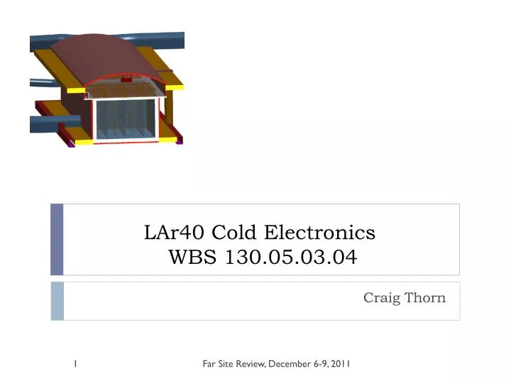
LAr40 Cold Electronics WBS 130.05.03.04 Craig Thorn Far Site Review, December 6-9, 2011
Outline • Scope & Requirements • Electronics specifications • Technical overview • Data rates • Zero-suppression • Electronics overview • Front-end (analog) ASIC • Digital (ADC, buffer, mux) ASIC • Cryogenic operation of CMOS ASICs • Electronics details and specifications • Schedule • Summary Far Site Review, December 6-9, 2011 Craig Thorn
Scope & Requirements • Scope: Can use WBS definitions (http://lbne2-docdb.fnal.gov:8080/cgi-bin/ShowDocument?docid=2163) for scope. Note that WBS#’s are out of date, also be sure text reflects current reference design choice. • Requirements: Get from Anne Heavey, DOORS output. (http://lbne2-docdb.fnal.gov:8080/cgi-bin/ShowDocument?docid=3747) Anne should have the outputs by Dec. 1st.) Far Site Review, December 6-9, 2011 Craig Thorn
Electronics Parameters Far Site Review, December 6-9, 2011 Craig Thorn
Total Event Rate For Noise With Zero-suppression • White (Series) Noise: SNR • Noise is 600 e rms • MIP is 10000 e (1 attn length , 5 mm spacing) • Threshold at 0.3 MIP: noise is 5 sigma • (for these conditions 0.1% of points on a MIP track are lost) • Probability of > 5 sigma is 2.8 x 10⁻⁷ • Read nearest neighbor wires + 2 leading & trailing samples • Rate per APA is 3 x 5 x 2560 x 150 kHz x 12 x 2.8 x 10-7 = 0.02 Mb/s Far Site Review, December 6-9, 2011 Craig Thorn
Practical Maximum Data Rate of LAr20 Radioactive contaminants • Ar39: Mean beta energy of 220 keV, endpoint 565 keV, 1.4 kBq/m3 • Kr85: Mean beta energy of 251 keV, endpoint 687 keV, 0.16 – 0.48 kBq/m3 • K40, Co60, Th232, U238: in construction materials, gammas only, atten length <15 cm • Arspallation by cosmics: no cross section data, but not significant in WARP data The energy spectrum observed with the 2.3 liter WARP detector (Data) can be reproduced by an internal component dominated by Ar39 and Kr85b emission inside the liquid argon. an external component dominated by interactions of g-rays coming from U238, Th232, Co60 and K40 radioactivity of the materials surrounding the liquid argon P. Benetti et al., NIM A 574 (2007) 83 Far Site Review, December 6-9, 2011 Craig Thorn
Practical Maximum Data Rate of LAr20 Radioactive contaminants • Ar39 • Decay rate is 122 kHz/APA • Mean ionization is ~0.3 MIP • Threshold @ 0.5 MIP, detected rate is 34 kHz • Mean range of betas is 0.28 mm • Read 3 wires and 10 samples • Mean rate is 3 x 8 x 34,000 x 12 = 9.8 Mb/s • Kr85 • Decay rate is ~28 kHz/APA • Mean ionization is ~0.4 MIP • Threshold @ 0.5 MIP, detected rate is 8 kHz • Mean range of betas is 0.39 mm • Read 3 wires and 5 samples • Mean rate is 3 x 8 x 8,000 x 12 = 2.3 Mb/s • Co60 • Only near SS APA frames since attenuation length is ~10 cm • add ~0.2Mb/s (range of Compton electron is 1.3 cm) Calculation of 220 keV electrons in LAr from CASINO www.gel.usherbrooke.ca/casino/index.html Far Site Review, December 6-9, 2011 Craig Thorn
Data Rates - Summary • Zero-suppression at FE reduces total volume of data to transmit • Buffering on FE ASIC allows data to be transmitted at lower rate than sampling rate • Readout rate must be high enough to avoid event “collisions” in one FE buffer • With optimal zero-suppression, radioactivity, cosmics, and series FE noise give rates of • 9.8 Mb/s for Ar39 betas • 2.3 Mb/s for Kr85 betas • 0.6 Mb/s for Co60, Th & U gammas • 0.02 Mb/s for FE series noise* • 0.8 Mb/s for cosmic muons (1 Gb/s near surface**) • Total is ~14 Mb/s (2 Gb) per APA at 800 (0) feet (cf. limit of 300Mb/s for copper, 3Gb/s for optical transmission per line) • *For an enc of 600 RMS e-, a threshold at 3000 e- and 1 us shaping (zero-crossing rate of 150kHz). For a 1/e drift time of 2.4 ms, a drift of 3.7 m and a wire pitch of 5 mm, this threshold is 0.3 MIP. • **Cosmic muon rate is 12 kHz (26 muon per drift, mean track length 2 m) Far Site Review, December 6-9, 2011 Craig Thorn
Zero Suppression – APA Trigger • Trigger derived from the logic OR of all collecting wires on an APA • All channels on an APA continuously writing to the buffer until no signal from any collecting wire • Baseline samples are compacted into smaller words (4bits) • Not efficient: little data reduction • Data volume is not sensitive to “noise” (thermal, induced, radioactivity, cosmics, …) Far Site Review, December 6-9, 2011 Craig Thorn
Zero Suppression – Chip Trigger • Trigger derived from the logic OR of all channels in a chip • All channels on a chip continuously writing to the buffer until no signal from any channel of a chip • Baseline samples are compacted into smaller words (4bits) • Data volume is sensitive to “noise” Far Site Review, December 6-9, 2011 Craig Thorn
Zero Suppression – Channel Trigger • Trigger is derived from a single channel • Write enable is applied to the i, i+1, and i-1wires to cover any shared, below threshold signals • Read ahead and after the write enable gate to capture the below threshold leading/trailing edges of a waveform • Minimum data volume • Data volume is less sensitive to “noise” Far Site Review, December 6-9, 2011 Craig Thorn
FEE Design Guidelines & Constraints some factors relevant to the design of final in-LAr readout architecture back-end redundancy lifetime power dissipation compression sparsification neighboring smart threshold derandomization(deep memory) reliability zero suppression low multiplexing, low clock frequency ↕ (conflict) high multiplexing, high clock frequency flexibility number of feed-throughs dead time token-passing (design option) programmability (design, operation) Far Site Review, December 6-9, 2011 Craig Thorn
LAr TPC - Cold CMOS Electronics Block Diagram – Lar40 Reference Design Far Site Review, December 6-9, 2011 Craig Thorn
LAr TPC - Cold CMOS Electronics Block Diagram – LAr40 Alternate Design Far Site Review, December 6-9, 2011 Craig Thorn
LAr TPC Front-End ASIC • 16 channels • charge amplifier (adj. gain) • high-order filter (adj. time constant) • ac/dc, adjustable baseline • test capacitor, channel mask • ADC (12-bit, 2 MS/s) • compression, discrimination • multiplexing and digital buffering • LV or CM digital interface • pulse generator, analog monitor • temperature sensor • LAr environment (> 20 years at 88K) • estimated total size ~ 6 x 8 mm² • estimated power ~ 10 mW/channel
Analog ASIC • 16 channels • charge amplifier, high-order filter • adjustable gain: 4.7, 7.8, 14, 25 mV/fC • (charge 55, 100, 180, 300 fC) • adjustable filter time constant • (peaking time 0.5, 1, 2, 3 µs) • selectable collection/non-collection mode • (baseline 200, 800 mV) • selectable dc/ac coupling (100µs) • rail-to-rail analog signal processing • band-gap referenced biasing • temperature sensor (~ 3mV/°C) • 136 registers with digital interface • 5.5 mW/channel (input MOSFET 3.9 mW) • single MOSFET test structures • ~ 15,000 MOSFETs • designed for room (300K) and cryogenic (77K) operation • technology CMOS 0.18 µm, 1.8 V Far Site Review, December 6-9, 2011 Craig Thorn
Signal Measurements Bandgap Reference variation ≈ 1.8 % Temperature Sensor ~ 2.86 mV / °K Pole-zero cancellation at 77K to be addressed in next revision Adjustable gain, peaking time and baseline maximum charge 55, 100, 180, 300 fC Far Site Review, December 6-9, 2011
Analog ASIC - Signal Measurements Warm tests for MicroBooNE Crosstalk < 0.7% Noise ~ 250e- w/o Cdet w. tp=1μs @RT Noise < 1000e-w. Cdet=150pF & tp=1μs @ RT Far Site Review, December 6-9, 2011
FEE ASIC Evaluation Noise, Gain, and Shaping Time Far Site Review, December 6-9, 2011
Analog ASIC - Noise Measurements Layout Detail Qmax=300fC Input MOSFET L = 270 nm W = 10 mm (50µm x 200) gm,77K ≈ 90 mS (11 Ω) gm,300K ≈ 45 mS (22 Ω) Input Line L ≈ 1 mm W = 3.5 µm (M3 + M4) R77K ≈ 3 Ω R300K ≈ 12 Ω Dynamic Range > 3,000 • Measurements affected by: • input line parasitic resistance • ~ 150 e- at 77 K (~ 590 e- at 300K ) • addressed in next revision • CINdielectric noise (not present in wire) • ~ 60 e- at 77 K ASIC version #3 designed and fabricated, currently being tested
Issues Addressed in Version 2 • Analog front-end • input MOSFET optimization → MOSFET width doubled • noise from resistance of input lines → line width doubled • Start-up failures in some bias circuit → start-up circuits added • (due to new BGR biasing circuits) Craig Thorn
Residual Issues in Version 2 • CMP damage in AC/DC circuit (found in a few samples) • Some packaging issues • DC PSR can be improved no baseline stabilization possible, due to constraint on measurement time Far Site Review, December 6-9, 2011 Craig Thorn
CMP Damage DC Only possible explanation: high series resistance (up to open) metal 5 metal 6 AC metal 5 interconnect line switch to buffer (metal 6) risk of CMP damage from filter Resistor Capacitor 280µm 1,100µm
CMP Damage Damage due to discharge from Chemical-Mechanical Polishing (CMP) during fabrication DC damaged channel good channel good channel damaged channel Far Site Review, December 6-9, 2011 Craig Thorn
FE ASIC Version 3 LArASIC3 LArASIC2 size 6010 x 5707 µm² bias circuit for high PSR LArASIC3 sent for fabrication on July 25th Received and under evaluation Far Site Review, December 6-9, 2011 Craig Thorn
ADC - Architecture Clockless low power ADC stage Demonstrated in ASIC for SNS, see De Geronimo, et al., IEEE Trans NSS, 54 (2007) 541 • Current mode ADC • dual stage6-MSBs in 150ns, 6-LSBs in 250ns • single trigger conversion per stage • 12-bit resolution • 2 MS/s conversion rate • power dissipation 3.6 mW at 2 MS/s • power-down option for low rate applications • wake up in few tens of ns • layout size: 0.23 mm x 1.25 mm ADC cell Far Site Review, December 6-9, 2011 Craig Thorn
ADC - Preliminary Results 300 K 16-channel ADC+buffer 6mm 77 K 4.3 mm ADC output - 1.4 V sine ADC output - 500mV dc σ=1.1LSB • operation verified at room and cryogenic temperatures • differential non-linearity limited by timing design error in control circuit • integral non-linearity limited by mismatch (linear → common centroid) Craig Thorn ASIC revision designed and fabricated; under evaluation
Schedule (install by others) • Schedule provided by Ken CD-1: 6/2012 CD-0: 1/2010 CD-2: 9/2013 CD-3: 12/2014 Designs Beneficial Occupancy: 10/2018 Construction Checkout Far Site Review, December 6-9, 2011 Craig Thorn
Milestones Far Site Review, December 6-9, 2011 Craig Thorn
Summary • CMOS performs better at cryogenic temperatures • Defined and predictable design for cryogenic T is possible • Low-noise at cryogenic T demonstrated • ENC < 1,000 e- at 200pF ~5mW/ch. • characterization and modeling of CMOS 180nm • Long lifetime at cryogenic T possible with guidelines • Critical building blocks - front-end & ADC - developed • Future work • Improve cryogenic static models • Optimize ADC • Merge, add zero-suppression & buffering, and finalize Far Site Review, December 6-9, 2011 Craig Thorn
Backup Information Far Site Review, December 6-9, 2011
ASIC Architecture ae re ck flgwi bias, pulser, logic, registers 8x analog 8x ADC thr/ trig cmp mem 3K mux 8:1 da taa,tab section a section b 8x analog 8x ADC thr/ trig cmp mem 3K mux 8:1 db tba,tbb • two independent 8-channel sections (a and b) • ADC max 2MS/s, 12-bit, calibrated for zero at baseline • mem can store one full-depth event (3K) per channel wo • da, db = data out • taa, tab, tba, tbb = triggers in/out (edge channels) • ae = acquisition enable (sync/reset acquisition at positive edge) • re = readout enable • ck = clock 32 or 64 MHz • rck (readout clock) 32 or 64 MHz • tck (timestamp & ADC clock) 2MHz • cck (test pulse clock) 8 kHz • wck (write clock) 8 MHz • flg = flag (full indicator, stops acquisition, restarts at 3/4 buffer empty) • wi, wo = configuration in/out • event stored in mem if: (i) above threshold or (ii) external trigger from neighbor (or FPGA)
Data Format max block size 4096-bit 0 (16) amplitude data time2 (10) time1 (10) addr (12) 1 (16) id (4) end start • variable block length, max 4096 bit • block-start: 16 ones • address 12-bit • 5-bit hard-assigned + 7-bit soft-assigned • all 0 and all 1 not allowed • timestamp 20-bit (2 x 10-bit) • associated to threshold crossing • Gray-code, 500 ns (2 MHz), ~500 ms full scale • all 0 and all 1 not allowed • block id (same timestamp) 4-bit • resets at each new timestamp • all 0 and all 1 not allowed • amplitude data 14-bit or n-bit • compress if below compression-threshold (programmable) • first bit: compression id (0 = compressed data, 1 = full data) • second bit: polarity (0 = negative, 1 = positive) • next bits: amplitude (12 for uncompressed, n-2 for compressed) • max amplitude length 4096 - 68 = 4028 bit (~288x14-bit) • can be broken to next block as needed • all 0 and all 1 not allowed • block-end: 16 zeros Craig Thorn
Cost Estimate Far Site Review, December 6-9, 2011 Craig Thorn
Labor vs M&S Far Site Review, December 6-9, 2011 Craig Thorn