Download
1 / 40
481 likes | 816 Vues
What you need to test an IC ?. (1) Power Supply/Current Meter. VDD. I dd. DUT. What you need to test an IC ?. (2) Signal Generator. VDD. DUT. in. What you need to test an IC ?. (3) Oscilloscope/Logic Analyzer. VDD. DUT. out. What you need to test an IC ?.

E N D
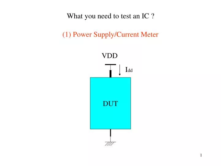
What you need to test an IC ? (1) Power Supply/Current Meter VDD Idd DUT
What you need to test an IC ? (2) Signal Generator VDD DUT in
What you need to test an IC ? (3) Oscilloscope/Logic Analyzer VDD DUT out
What you need to test an IC ? (4) Voltage Source/Current Meter VDD DUT Iin in I-meter + Volt _
What you need to test an IC ? (5) Current Source/Voltage Meter VDD DUT Vout out V-meter + Current _
Basic Request for IC Tester Combine following function in Test Machine (1) Power Supply/Current Meter (2) Signal Generator (3) Oscilloscope/Logic Analyzer (4) Voltage Source/Current Meter (5) Current Source/Voltage Meter
DPS Power Driver PEC Pin Driver PMU DUT V-Source I-Meter in1 in2 Comparator out1 out2 PMU I-Source V-Meter
DPS Power Driver 1. Provide device under test with operating power. 2. Power supply voltage can be programming. @2V, @4V, @8V, @10V Range 3. Ability for supply current measurement function. @1uA, @10uA, @100uA, @1mA, @10mA,@100mA, @1A Range 4. Four independent DPS source in System.
PEC Pin Driver Comparator 1. Provide DUT with specified level stimulus signals. 2. Provide two rail comparators to capture output signal. 3. Stimulus/Capture are controlled by “Pat”, “TG”, “Format” and “Levels” . All are programmable to fit application. 4. 256 independent channels source in System.
PMU V/I Source I/V Meter 1. Provide device pins with Voltage/Current source. And ability for Current/Voltage measurement. FVMI and FIMV mode. 2. Voltage Source/Measurement function. @2V, @4V, @8V, @10V Range 3. Current Source/Measurement function. @1uA, @10uA, @100uA, @1mA, @10mA,@100mA, @1A Range 4. Four independent PMU source in System.
Open/Short(Continuity) Test FORMAT_SET( OS_TEST ); ALLPINS = ( NRZ, NRZ, NORMAL); END_FS; TIMING_SET( FASTCON, 20.00us ); ALLPINS = F( 0.00ns, 100.00ns ), IO( 0.00ns, 100.00ns ), STB( 19.00us, 19.5us ); END_TS; LEVEL_SET( OS_TEST_LVL ); ALLPINS = VIH(3.60 V), VIL( 0.0 V), VOH(-0.2 V), VOL(-1.0 V), IOH(200uA), IOL(200uA), VCM(-2.00 V); END_LS; PLAN(cont); DISCONNECT(ALLPINS, PMU); DPS_FV(DPS1, 0.000nV, V1I6); SET_REF_LEVEL( OS_TEST_LVL ); SET_PIN_LOW( ALLPINS ); CONNECT(ALLPINS, DCL); WAIT(3ms); PMU_FIMV(ALLPINS, -100.000uA, V1I4, -1.000V, -200.000mV, 0.000ms, OFF, ON ); SET_FORMAT(INIT); DISCONNECT(ALLPINS, PMU); END_PLAN;
DPS force 0.0V VDD DCL DCL IN_1 OUT_1 0.0V . . . . . . . 0.0V PMU PMU Normal value = +0.6V(100uA) or -0.6V(-100uA) DCL DCL IN_2 OUT_2 . . . . . . . 0.0V 0.0V PMU PMU GND
DPS force 0.0V VDD DCL DCL IN_1 OUT_1 0.0V . . . . . . . 0.0V PMU PMU Pin opened DCL DCL IN_2 OUT_2 . . . . . . . 0.0V 0.0V PMU PMU Measured value = +2.5(100uA@V1) or -2.5(-100uA @V1) GND
DPS force 0.0V VDD DCL DCL IN_1 OUT_1 0.0V . . . . . . . 0.0V PMU PMU Measured value = 0.0V Pin to pin short DCL DCL IN_2 OUT_2 . . . . . . . 0.0V 0.0V PMU PMU GND
Functional Test Connect to DPS DUT VOH VIH VCC 7404 CMP_H 0/1 010101 HLHLHL A B CMP_L ON/OFF GND VIL VOL Connect to GND A Truth table pattern A B 0 1 1 0 /* AB */ * 0H *; * 1L *; B TPDhl TPDlh
What is Pattern ? What is TG ? What is FORMAT ? What is Level ?
Pattern • Pattern is the “truth table”. Symbol Main information in the period 0 • Force 0 1 • Force 1 H • Compare High L • Compare Low X • No Drive / Don’t care output Z • No Drive / Compare Tri-state O • Force 0 + Compare Low o • Force 0 + Compare High I • Force 1 + Compare High i • Force 1 + Compare Low
TG (timing Generator) • FTG define the timing of input signal goes 1 and goes 0 • IOTG define the timing of input signal turns on and off • STB define the timing to capture output signal F IO STB
Format • Format is waveform type. • F- Format.(control goes 1/0) Format Remark NRN Non Return to Zero ( Once goes 1, not back to 0 in period) RZ Return to zero ( Once goes 1, back to 0 later in period) RTO Return To One (Once goes 0, back to 1 later in period) NXOR Surround by compliment @1 FH Static 1, not pattern controlled FL Static 0, not pattern controlled
IO- Format.(control drive on/off) Format Remark NRN Non Return to Zero ( Once drive on, not back to off in period) RZ Return to zero ( Once drive on, back to off later in period) RTO Return To One (Once drive off, back to on later in period) NXOR Surround by compliment @2 DON Driver always turns on , not pattern controlled DOFF Driver always turns off , not pattern controlled • L- Format.(control load on/off) Format Remark NORMAL Follow IO ( IO turns on , load is off. IO turns off, load is on automatically) LON Load always on , not pattern controlled LOFF Load always off , not pattern controlled
F and IO Format Function Block Function Description Application NRZ Block PAT D Q ( D Flip-Flop ) CLK - Data bus - Addr bus DFF. D = PAT DFF. CLK = TG NRZ Out = DFF. Q NRZ Out TG RZ Block PAT AND RZ Out . RZ Out = PAT TG - Clock pin - Control pin(high active) TG RTO Block PAT OR - Clock pin - Control pin(low active) RTO Out RTO Out = TG + PAT TG INV NXOR Block PAT XOR - Addr bus (access test) INV NXOR Out NXOR Out = TG PAT TG
PAT 0 1 1 0 0 TG NRZ RZ RTO NXOR Combine Pattern, TG and Format
Level • Level defines the Input/Output DC level Level Remark VIH The voltage when pin driver goes 1 VIL The voltage when pin driver goes 0 VOH The High threshold voltage for of DUT output VOL The low threshold voltage for of DUT output IOH The current load when DUT output High IOL The current load when DUT output Low VCM The communication voltage for Tri-State or switching IOH/IOL
Pin Driver Block Diagram F_PAT MUX NRZ F_TG VIH RZ Transmission gate Pin Drive RTO F_CTRL NXOR IO control (Fixed High) 1 VIL (Fixed Low) 0 3 F_FORM_SEL D_PAT MUX NRZ D_TG (IO_TG) RZ RTO D_CTRL NXOR (Drv On) 1 (Drv Off) 0 3 D_FORM_SEL (IO_FORM_SEL)
F_CTRL, D_CTRL and Level Goes 0 Goes 1 F_CTRL Drive on Drive off D_CTRL VIH Hi-Z VIL Strobe
PEC Block Diagram -- Pin Electronics VIHx (From reference buffer) 1 DCL F_CTRLx PE_Px (To Back plane connector, then to DUT via Flat Cable) 0 VILx PMU (From reference buffer) D_CTRLx IOLx VOHx Comp PEH_Px (From reference buffer) (To Format/Response Chips) L_CTRLx Comp PEL_Px IOHx VOLx D1 D2 (To Format/Response Chips) (From reference buffer) GND VCMx (From reference buffer)
Fast Continuity Test FORMAT_SET( OS_TEST ); ALLPINS = ( NRZ, NRZ, NORMAL); END_FS; TIMING_SET( FASTCON, 20.00us ); ALLPINS = F( 0.00ns, 100.00ns ), IO( 0.00ns, 100.00ns ), STB( 19.00us, 19.5us ); END_TS; LEVEL_SET( OS_TEST_LVL ); ALLPINS = VIH(3.60 V), VIL( 0.0 V), VOH(-0.2 V), VOL(-1.0 V), IOH(200uA), IOL(200uA), VCM(-2.00 V); END_LS; *XXXXXXXXXX* TS = FASTCON; *Z000000000*; *0Z00000000*; *00Z0000000*; *000Z000000*; *0000Z00000*; *00000Z0000*; *000000Z000*; *0000000Z00*; *00000000Z0*; *000000000Z*; *XXXXXXXXXX* Halt; PLAN(fast_con); DISCONNECT(ALLPINS, PMU); CONNECT(ALLPINS, DCL); SET_FORMAT(OS_TEST); SET_REF_LEVEL(OS_TEST_LVL); DPS_FV(DPS4, 0.000nV, V1I6); BURST_PATTERN(OS); SET_FORMAT(INIT); DISCONNECT(ALLPINS, PMU); END_PLAN;
DPS force 0.0V 1 (1) VDD VOH = 1.0V (-0.2V) To Response block (compare Z) 1 (1) IN_1 To Response block DCL 0.0V VOL = 0.2V (-1.0V) 100uA~200uA 0.6V (-0.6V) IN_2 VCM = 2.0V (-2.0V) DCL GND 100uA~200uA
DPS force 0.0V 0 (1) VDD VOH = 1.0V (-0.2V) To Response block (compare Z) 1 (0) IN_1 To Response block DCL 0.0V VOL = 0.2V (-1.0V) 100uA~200uA 2.0V (-2.0V) IN_2 VCM = 2.0V (-2.0V) DCL GND 100uA~200uA
DPS force 0.0V 1 (0) VDD VOH = 1.0V (-0.2V) To Response block (compare Z) 0 (1) IN_1 To Response block DCL 0.0V VOL = 0.2V (-1.0V) 100uA~200uA 0.0V (-0.0V) IN_2 VCM = 2.0V (-2.0V) DCL GND 100uA~200uA
D[0..7] Q[0..7] 74HC273 CLK /CLR D[0..7] Q[0..7] CLK /CLR 1 (F-RTO) /CLR (IO-NRZ) A B C D (F-NRZ) D (IO-NRZ) (F-NRZ) Q(output) (IO-NRZ) A B C D (F-RZ) CLK (IO-NRZ)
A[0..14] D[0..7] 62256 /OE /WE ADDR[0..14] DATA[0..7] /OE /WE 1 (F-NRZ) /OE (IO-NRZ) (F-NRZ) ADDR (IO-NRZ) A A+1 A+2 A+3 (F-NRZ) DATA(input) (IO-NRZ) D(A) D(A+1) D(A+2) D(A+3) (F-RTO) /WE (IO-NRZ)
DB[0..11] DAC Digital to Analog Converter /CS /WE /LDAC DB[0..11] VOUT /CS /WE /LDAC (F-NRZ) /CS (IO-NRZ) (F-NRZ) DATA(input) (IO-NRZ) D(0) D(1) D(2) D(3) (F-RTO) /WE (IO-NRZ) (F-RTO) /LDAC (IO-NRZ)
A[0..14] D[0..7] 62256 /OE /WE ADDR[0..14] DATA[0..7] /OE /WE access time 0 (F-NRZ) /OE (IO-NRZ) (F-NXOR) ADDR (IO-NRZ) A1 A1 A1 A2 A2 A2 A3 A3 (F-NRZ) DATA(output) (IO-NRZ) D(A1) D(A1) D(A1) D(A2) D(A2) D(A2) D(A3) (F-NRZ) /WE (IO-NRZ) 1
A[0..7] B[0..7] 74HC245 /G DIR A[0..7] B[0..7] /GATE DIR 1 (F-NRZ) /GATE (F-NRZ) A (IO-RZ) A B A B A B A B A (F-NRZ) B (IO-RZ) A B A B A B A B A (RZ) DIR A IO_TG B IO_TG
ISB = ISBexp - (Vx/Rx) - (Vy/Ry) DPS FV=VDD VDD Pull high resistor = Rx VIH = VDD + Vx Ix = Vx/Rx IN_1 DCL VIL Pull high resistor = Ry VIH = VDD + Vy Iy = Vy/Ry IN_2 DCL VIL Note : Vx,Vy might be +/-20 mV deviation if Rx,Ry are 20K Ohm, ISB will have 1uA/pin deviation GND
ISB = ISBexp DPS FV=VDD VDD Pull high resistor = Rx VIH = VDD + Vx Ix = 0 IN_1 DCL VIL Pull high resistor = Ry VIH = VDD + Vy Iy = 0 IN_2 DCL VIL Note : Vx,Vy might be +/-20 mV deviation GND
DPS FV=VDD VDD Pull high resistor = Rx Rx ~= V_drop/Ix Ix IN_1 PMU FV = VDD - V_drop PMU Pull high resistor = Ry Ry ~= V_drop/Iy Iy IN_2 PMU FV = VDD - V_drop PMU GND Check pull-high resistor by PMU_FVMI to get current value. Set PMU force value to be a little voltage drop(ex. 0.1 or 0.5V) lower than VDD. Pull-high resistance can be roughly calculated by Voltage_drop/Current_value.
PLAN( Low_Func); . . BURST_PATTERN(Demo); . . END_PLAN; PATTERN( Demo, Header1, F_Fumc); *000111XXXXXXXXXX* TS= TS1; *000111XXXHLHLXXX*; *000111XXXHLHLXXX*; *000111XXXHLHLXXX*; *000111XXXHLHLXXX*; *000111XXXHLHLXXX* Halt; END_PATTERN; Better one PLAN( Low_Func); . . SET_FORMAT(F_Func); BURST_PATTERN(Demo); . . END_PLAN; PATTERN( Demo, Header1); *000111XXXXXXXXXX* TS= TS1; *000111XXXHLHLXXX*; *000111XXXHLHLXXX*; *000111XXXHLHLXXX*; *000111XXXHLHLXXX*; *000111XXXHLHLXXX* Halt; END_PATTERN;