Download
1 / 33
330 likes | 470 Vues
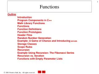
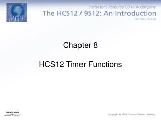
TPU: time functions. Input event detection Output event generation Pulse-rate sensing Pulse-rate modulation Pulse-width modulation. TPU. TPU. Serial Comm. ADC. ADC. IMB. RCPU. U-bus. U-bus System Interface Unit (USIU). SRAM. SRAM. L-bus. Time Processor Unit (TPU). TPU.

E N D
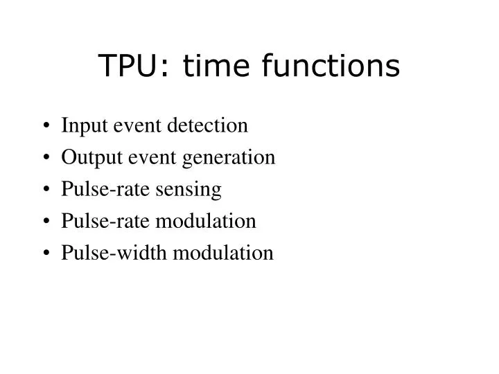
TPU: time functions • Input event detection • Output event generation • Pulse-rate sensing • Pulse-rate modulation • Pulse-width modulation
TPU TPU Serial Comm ADC ADC IMB RCPU U-bus U-bus System Interface Unit (USIU) SRAM SRAM L-bus Time Processor Unit (TPU)
TPU Controls 16 channels (available as pins). Can observe events on these channels (input). Can generate events on these channels (output). Events: transitions to indicate some state.
16-bit counters Memory-mapped interface channels TCR1 IMB3 System Config. Chan 0 Chan 1 Chan 15 TCR2 Micro- Engine Channel control Parameter RAM TPU
TPU Timers Two timers: TCR1 & TCR2 -- 16 bits each All channel events are created or captured w.r.t. a timer. TCR1 programmed in TPUMCR. TCR2 can be driven by an external clock.
8 9 0 1:2 TCR1P supv psck Clock prescalar 0: 32 1: 4 00: div by 1 01: div by 2 10: div by 4 11: div by 8 TPU Registers TPU Module Configuration Register: TPUMCR 0x30 4000
0:4 5:7 8:9 CIRL ILBS Channel interrupt request level: 0-7. TPU Control Registers TPU Interrupt Configuration Register (TICR) 0x30 4008
1 2 0 14 15 Ch 15 Ch 14 Ch 13 Ch 1 Ch 0 TPU Control Registers Channel Interrupt Enable Register (CIER) 0x30 400a 0: interrupt disabled 1: interrupt enabled
1 2 0 14 15 Ch 15 Ch 14 Ch 13 Ch 1 Ch 0 TPU Control Registers Channel Interrupt Status Register (CISR) 0x30 4020 Channel interrupt status: 0: interrupt not asserted 1: interrupt asserted
Channel 0 Capture the time of the transition Channel Programming 16 predefined functions. Input Capture: capture one or multiple transitions on an input pin.
REF_TIME1 offset Ref_Time = REF_TIME1 + offset Channel Programming Program as an output channel. Output Compare: generate an event on the output: a single output transition, a single pulse, or a continuous 50% duty cycle pulse train.
0x30 4012: Channel Function Select Register 3 (CFSR3) 0x30 400c: Channel Function Select Register 0 (CFSR0) 0x30 400e: Channel Function Select Register 1 (CFSR1) 0x30 4010: Channel Function Select Register 2 (CFSR2) Ch 15 Ch 11 Ch 3 Ch 7 Ch 6 Ch 10 Ch 14 Ch 2 Ch 1 Ch 13 Ch 9 Ch 5 Ch 8 Ch 0 Ch 12 Ch 4 Channel Initialization Choose channel function: Code for IC: 0xA Channel function code for OC: 0x4
Channel W 0x3041W0 Channel Control (9 bits) 0x3041W2 0x3041W4 MAX_COUNT 0x3041W6 TRANS_COUNT 0x3041W8 FINAL_TRANS_TIME 0x3041Wa LAST_TRANS_TIME Input Capture Parameters
Input Capture/Transition Counter Input Parameters: MAX_COUNT: The TPU raises an interrupt after counting as many events as MAX_COUNT. Output Parameters: TRANS_COUNT: current count of captured transitions. FINAL_TRANS_TIME: Timer time when the final transition (MAX_COUNTth) is captured. LAST_TRANS_TIME: Timer time when the last transition (TRANS_COUNTth) is captured.
Memory Map of Parameters Channel 0: MAX_COUNT: 0x30 4104 TRANS_COUNT: 0x30 4106 FINAL_TRANS_TIME: 0x30 4108 LAST_TRANS_TIME: 0x30 410A General Channel Y: MAX_COUNT: 0x30 41Y4 TRANS_COUNT: 0x30 41Y6 FINAL_TRANS_TIME: 0x30 41Y8 LAST_TRANS_TIME: 0x30 41YA
f2 02 12 22 f4 04 14 24 06 16 26 f6 f8 08 28 08 0a 1a 2a fa fc 2c 1c 0c 0e 2e 1e fe 10 f0 00 20 P1 P1 P1 P1 P2 P2 P2 P2 P3 P3 P3 P3 P4 P4 P4 P4 P5 P5 P5 P5 P6 P6 P6 P6 P7 P7 P7 P7 P8 P8 P8 P8 General Parameter Memory Map 0x3041 Ch 0 Ch 1 Ch 2 Ch 15
7:10 11:13 14:15 0:6 TBS PAC PSC Pin State Control 11:do not force any state input pin 01: force high 10: force low Time Base Selection 00xx: input channel 000x: capture TCR1 001x: capture TCR2 Pin Action Control 000:do not detect trans. 001:detect rising edge 010:detect falling edge 011:detect either edge 1xx:do not change PAC Channel Control Options Part of channel initialization
0x30 401c: Channel Priority Register 0 (CPR0) 0x30 401e: Channel Priority Register 1 (CPR1) Ch 15 Ch 3 Ch 11 Ch 7 Ch 10 Ch 6 Ch 2 Ch 14 Ch 9 Ch 13 Ch 1 Ch 5 Ch 4 Ch 0 Ch 12 Ch 8 Channel Priority Choose channel priority: 0:disable; 1:low; 2: medium; 3: high
0x30 4018: Host Service Request Register 0 (HSRR0) 0x30 401a: Host Service Request Register 1 (HSRR1) Ch 15 Ch 3 Ch 11 Ch 7 Ch 10 Ch 6 Ch 2 Ch 14 Ch 9 Ch 13 Ch 1 Ch 5 Ch 4 Ch 0 Ch 12 Ch 8 Channel Function Activation After initializing channel, the channel function is activated by host service request, which can be further specialized through host sequence.
0x30 4014: Host Sequence Register 0 (HSQR0) 0x30 4016: Host Sequence Register 1 (HSQR1) Ch 15 Ch 3 Ch 11 Ch 7 Ch 2 Ch 6 Ch 14 Ch 10 Ch 9 Ch 5 Ch 1 Ch 13 Ch 12 Ch 4 Ch 0 Ch 8 Host Sequence Transition sequencing: x0: single shot x1: continual
Typical Initialization Sequence • Disable the channel before programming it • CPR[ch] 00 (channel priority – disabled) • Assign the channel function • CFSR[ch] 0xA (for input capture/ITC) • Program the function parameters • MAX_COUNT=1 for input capture • Channel control: TBS: 000x (input channel; capture TCR1); PAC: 001 (detect rising edge); PSC: 11 (do not force) • Host sequence single shot. Write 00 into HSQRR[ch]. • etc. • Initialize host service (activate the channel): • HSRR[ch] 01 (initialize TCR mode) • Enable the channel: • CPR[ch] 01, 10, 11
0x30 401a: Host Service Request Register 1 (HSRR1) Ch 7 Ch 3 Ch 6 Ch 2 Ch 5 Ch 1 Ch 4 Ch 0 Shared Register Modification 00: Host service complete by TPU channel 01: Initialize TCR mode by CPU Program Modification of HSRR involves read-modify-write: lhz r6, 0x401a(r5) //read andi r6, r6, 0xfffc // modify (write %01 to HSRR[ch0]) ori r6, r6, 0x1 sh r6, 0x401a(r5) // write Does it work? How many independent potential writers into HSRR1?
00 00 00 00 00 00 00 11 00 00 11 11 10 01 00 10 10 01 01 00 00 00 00 00 lhz r6, 0x401a(r5) //read andi r6, r6, 0xfffc // modify (write %01 to HSRR[ch0]) ori r6, r6, 0x1 sth r6, 0x401a(r5) // write Shared Register Modification Contd. We don’t really know what happens to ch 1-7 fields while we modify ch 0 field.
00 00 Ch 3 Ch 7 Ch 2 00 11 Ch 6 Ch 5 10 00 Ch 1 Ch 0 00 00 Ch 4 Shared Register Modification Contd. Solution: into ch 1-7 fields, write something we are definitely not supposed to write. 00 is written by only the TPU, no CPU program should legitimately write that value. li r6, 0x1 //00 00 00 00 00 00 01 sth r6, 0x401a(r5) 01 Write guard logic only allows 01, 10, 11 to go through!
REF_TIME1 offset Ref_Time = REF_TIME1 + offset Pin state forced to high (immediate output selected). REF_TIME1 offset Ref_Time = REF_TIME1 + offset The pin state is not forced into an immediate output. Output Compare (OC)
Output Compare (OC) • OC parameters specified by the CPU program: • REF_TIME1 as a pointer into the parameter space • of any of the 16 channels. • Parameter address space: 0x3041 00 – 0x3041 fe • Need to specify only 8-bits of address for REF_ADDR1. • OFFSET: a 16-bit quantity: 0x0 – 0x8000.
(REF_ADDR1) OFFSET REF_TIME = (REF_ADDR1) + OFFSET OC Programming Point REF_ADDR1 to 0x3041 ec (TCR1 value captured at this parameter address). OFFSET = 0x1000 with TCR1 resolution at 1 micro-s: 4.096 milli-s. Channel function code for OC: 0x4 CFSR[ch] 0x4
(REF_ADDR1) OFFSET REF_TIME = (REF_ADDR1) + OFFSET Output Compare OC initialization (host service request of 01 -- host initiated pulse mode) writes the current value: TCR1 0x3041 ec; TCR2 0x3041ee Program channel 0 for this pulse.
7:10 11:13 14:15 0:6 TBS PAC PSC Time Base Selection 01xx: output channel 0100: capture TCR1, match TCR1 0101: capture TCR1, match TCR2 0110: capture TCR2, match TCR1 0111: capture TCR2, match TCR2 1xxx: do not change TBS Pin State Control 11: do not force any state 01: force high 10: force low Pin Action Control 000: do not change pin state on match 001: high on match 010: low on match 011: toggle on match 1xx: do not change PAC OC Channel Control Options
Do not force initial state Capture TCR1, match TCR1 0100 011 11 (REF_ADDR1) Toggle on match OFFSET REF_TIME = (REF_ADDR1) + OFFSET OC Channel Control
(REF_ADDR1) OFFSET REF_TIME = (REF_ADDR1) + OFFSET Force high Capture TCR1, match TCR1 0100 010 01 Low on match OC Channel Control
Channel W Channel Control (9 bits) 0x3041W0 OFFSET 0x3041W2 0x3041W4 RATIO REF_ADDR1 0 REF_ADDR2 0 REF_ADDR3 0 0x3041W6 REF_TIME 0x3041W8 ACTUAL_MATCH_TIME 0x3041Wa Other OC Parameters We will write 0’s into RATIO, REF_ADDR2, and REF_ADDR3.
OC Output Parameters • When a channel is initialized for OC through a • service request of 01, REF_TIME is computed • as (REF_ADDR1) + OFFSET and placed in • parameter REF_TIME. • REF_TIME is the next time instant when an event would occur (and an interrupt is raised). • This is the match event: compare TCR1/2 with REF_TIME for a match. ACTUAL_MATCH_TIME is updated with the TCR1/2 time when the match is serviced (by raising an interrupt, and changing the level of the output channel).