Download
1 / 41
410 likes | 592 Vues
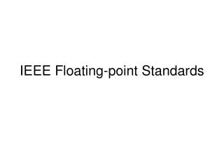
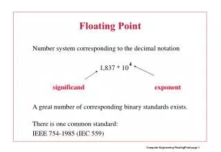
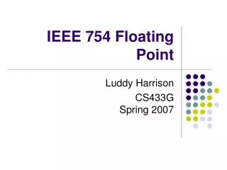
IEEE 754 Floating Point Standard. Normalized REAL Binary Number: ± 1.yyyyyyyyy x 2 eeee IEEE 754 (-1) S x ( 1 + F) x 2 E-127. s exponent+127 significand - 1. 1 bit E (8 bits) F (23 bits). Only Zero is F = 0 and E = 0

E N D
IEEE 754 Floating Point Standard Normalized REAL Binary Number: ±1.yyyyyyyyy x 2eeee IEEE 754 (-1)S x ( 1 + F) x 2E-127 s exponent+127 significand - 1 1 bit E (8 bits) F (23 bits) • Only Zero is F = 0 and E = 0 • Simplifies data exchange • Compare using integer processes • Accuracy and round-off & Overflow and Underflow
IEEE 754 Floating Point Standard Normalized REAL Binary Number: ±1.yyyyyyyyy x 2eeee Double Precision IEEE 754 (-1)S x ( 1 + F) x 2E-1023 s exponent+1023 significand - 1 1 bit E (11 bits) F (20 bits) significand – 1 (continued) F (32 bits)
Sequential Network Structures - Review Input Y1 Y2 Ym X1 X2 Xn Q1 Q2 Qm Combinational Logic Register Q Z1 Z2 Zk Clock Output clki Y Q Stability Condition
Flip - Flop with NOR Gates R Q = R+Q Q = S+Q S Present State RS Q 00 01 10 11 0 1 Next State Q
Flip - Flop with NOR Gates R Q = R+Q Q = S+Q S Present State RS Q 00 01 10 11 0 0 1 1 Next State Q
Flip - Flop with NOR Gates R Q = R+Q Q = S+Q S Present State RS Q 00 01 10 11 0 0 1 1 1 1 Next State Q
Flip - Flop with NOR Gates R Q = R+Q Q = S+Q S Present State RS Q 00 01 10 11 0 0 1 0 1 1 1 0 Next State Q
Flip - Flop with NOR Gates R Q = R+Q Q = S+Q S Present State RS Q 00 01 10 11 0 0 1 0 ? 1 1 1 0 ? Next State Q
D-latch R C Q Q D S D C Q
D-latch R C Q Q D S D C Q
D flip-flop D Q D Q D Q Output changes only on the trailing clock edge D D _ l a t c h l a t c h C C Q C D C Q
D flip-flop D Q D Q D Q Output changes only on the trailing clock edge D D _ l a t c h l a t c h C C Q C D C Q
Sequential Network Structures - Review Input Y1 Y2 Ym X1 X2 Xn Q1 Q2 Qm Combinational Logic Register Q Z1 Z2 Zk Clock Output clki Y Q Stability Condition
Five Components of Computers Memory Control Input Datapath Output Processor
Start by Building the Datapath • Access the Instruction from Memory • Access the Data from Registers • Perform the Instruction • Write the Result
PC Next PC Logic Address Instruction Memory Simplified Overview Instruction Access the Instruction from Memory
PC Next PC Logic Address Instruction Memory Simplified Overview Instruction Register File Access the Data from Registers
PC Next PC Logic Address Instruction Memory Simplified Overview Instruction Register File ALU Perform the Instruction
PC Next PC Logic Address Instruction Memory Simplified Overview Instruction Addr Register File Data Memory ALU Data Out Data In Write the Result
PC Next PC Logic Address Instruction Memory Simplified Overview Instruction Addr Register File Data Memory ALU Data Out Data In Timing Assumption
Basic Instruction Fetch PC + 4 PC Adder 4 PC Address M[PC] Instruction Instruction Memory
MIPS - Lite Consider the following instructions for implementation INSTRUCTION OP FUNCT R type add 0 32 subtract 0 34 AND 0 36 OR 0 37 set on less than 0 42 load word 35 na store word 43 na branch equal 4 na
R type Arithmetic Logic Instructions add rd, rs, rt R op rs rt rd shamt funct 6 5 5 5 5 6 • All R type Instructions • Read two registers addressed by rs and rt • Write one register addressed by rd • R[rs] + R[rt] R[rd] for add
Register File R e a d r e g i s t e r n u m b e r 1 R e g i s t e r 0 R e g i s t e r 1 M u R e a d d a t a 1 x R e g i s t e r n – 1 R e g i s t e r n R e a d r e g i s t e r n u m b e r 2 M u R e a d d a t a 2 x
Register File W r i t e C 0 R e g i s t e r 0 1 D • Note: we still use the real clock to determine when to write n - t o - 1 C R e g i s t e r n u m b e r d e c o d e r R e g i s t e r 1 D n – 1 n C R e g i s t e r n – 1 D C R e g i s t e r n D R e g i s t e r d a t a
n to 1 Decoder RA4 RA3 RA2 RA1 RA0 Multiplexor OOOO OOOOO ••• 31 0 1 R0i R1i Dri + • • R31i
Register File R e a d r e g i s t e r R e a d n u m b e r 1 d a t a 1 R e a d r e g i s t e r n u m b e r 2 R e g i s t e r f i l e W r i t e r e g i s t e r R e a d d a t a 2 W r i t e d a t a W r i t e
R type Arithmetic Logic Instructions add rd, rs, rt R op rs rt rd shamt funct 6 5 5 5 5 6 • All R type Instructions • Read two registers addressed by rs and rt • Write one register addressed by rd • R[rs] + R[rt] R[rd] for add
A L U c o n t r o l 5 R e a d r e g i s t e r 1 R e a d d a t a 1 5 R e g i s t e r R e a d Z e r o r e g i s t e r 2 n u m b e r s R e g i s t e r s D a t a A L U A L U 5 W r i t e r e s u l t r e g i s t e r R e a d d a t a 2 W r i t e D a t a d a t a R e g W r i t e a . R e g i s t e r s b . A L U Dataflow for R – type Arithmetic – Logical Instructions add rd, rs, rt Instruction R[rs] + R[rt] R[rd] rs rt rd 3 ALU is Combinational Logic
Load Word & Store Word ( I – type ) lw rt, imm16 (rs) or sw rt, imm16 ( rs) op rs rt imm16 lw # load word M[ R[rs] + sign_ext(imm16) ] R[rt] sw # store word R[rt] M[ R[rs] + sign_ext(imm16) ]
load word M[ R[rs] + sign_ext(imm16) ] R[rt] Registers Data Memory rs rt R1 R2 Rw Dw Dr1 Dr2 ALU Addr Dr Dw imm16 sign ext 32 16
store word R[rt] M[ R[rs] + sign_ext(imm16) ] Registers Data Memory rs rt R1 R2 Rw Dw Dr1 Dr2 ALU Addr Dr Dw imm16 sign ext 32 16
beq rs, rt, imm16 I -type op rs rt imm16 • Zero =1 iff rs - rt = 0 • If Zero = 1 • SUM (ShLt2[Sign_Ext(imm16)] + PC+4) PC • If Zero = 0 • PC+4 PC Zero (PC+4) + Zero SUM[ (ShLt2[Sign_Ext(imm16)])+PC+4] PC
Zero (PC+4) + Zero SUM[ (ShLt2[Sign_Ext(imm16)])+PC+4] PC Ex: imm16 is 1011 0000 0011 1001
Zero (PC+4) + Zero SUM[ (ShLt2[Sign_Ext(imm16)])+PC+4] PC Ex: imm16 is 1011 0000 0011 1001 Sign_Ext(imm16) is 1111 1111 1111 1111 1011 0000 0011 1001
Zero (PC+4) + Zero SUM[ (ShLt2[Sign_Ext(imm16)])+PC+4] PC Ex: imm16 is 1011 0000 0011 1001 Sign_Ext(imm16) is 1111 1111 1111 1111 1011 0000 0011 1001 ShLt2[Sign_Ext(imm16)] is 1111 1111 1111 11101100 00001110 0100
Zero (PC+4) + Zero SUM[ (ShLt2[Sign_Ext(imm16)])+PC+4] Zero =1 iff rs - rt = 0 PC PC+4 Sum to PC ALU Shift Left 2 branch equal imm16 sign ext 32 16
Zero (PC+4) + Zero SUM[ (ShLt2[Sign_Ext(imm16)])+PC+4] Zero =1 iff rs - rt = 0 PC PC+4 Sum to PC ALU branch equal Shift Left 2 ALU op Registers Zero rs rt R1 R2 Rw Dw Dr1 Dr2 ALU imm16 sign ext 32 16
P C S r c M A d d u x A L U A d d 4 r e s u l t S h i f t l e f t 2 R e g i s t e r s A L U o p e r a t i o n 3 R e a d M e m W r i t e A L U S r c R e a d r e g i s t e r 1 P C R e a d a d d r e s s R e a d M e m t o R e g d a t a 1 Z e r o r e g i s t e r 2 I n s t r u c t i o n A L U A L U R e a d W r i t e R e a d A d d r e s s r e s u l t M d a t a r e g i s t e r d a t a 2 M u I n s t r u c t i o n u x W r i t e m e m o r y D a t a x d a t a m e m o r y W r i t e R e g W r i t e d a t a 3 2 1 6 S i g n M e m R e a d e x t e n d Dataflow Review Fig 5.13 page 354


![Convert Decimal to Floating point number [IEEE 754]](https://cdn1.slideserve.com/1860729/convert-decimal-to-floating-point-number-ieee-754-dt.jpg)