Download
1 / 4
40 likes | 43 Vues
The full-fledged productivity of the semiconductor is mostly dependent on the robotic wafer handling industry. To trade the processed wafer with the unprocessed one is turning out to be a barricade in boosting the processing machinesu2019 performance without even measuring the time the process will take.

E N D
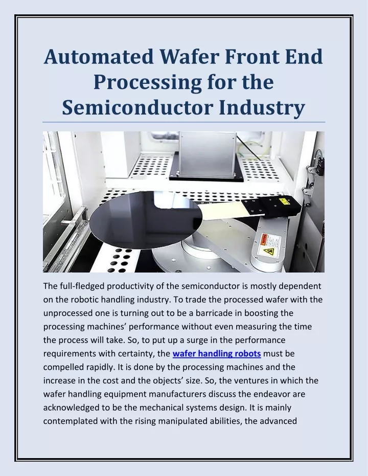
Automated Wafer Front End Processing for the Semiconductor Industry The full-fledged productivity of the semiconductor is mostly dependent on the robotic handling industry. To trade the processed wafer with the unprocessed one is turning out to be a barricade in boosting the processing machines’ performance without even measuring the time the process will take. So, to put up a surge in the performance requirements with certainty, the wafer handling robots must be compelled rapidly. It is done by the processing machines and the increase in the cost and the objects’ size. So, the ventures in which the wafer handling equipment manufacturers discuss the endeavor are acknowledged to be the mechanical systems design. It is mainly contemplated with the rising manipulated abilities, the advanced
control schemes practices, and the best app depicting wafer handling equipment via broad analysis of the wielding task with enlarging the case studies, mathematical modeling, simulation, and the on-site experiments. An integrated circuit is known to be a small but practical device enforcing various electronic functions. It generally depicts two parts, i.e., a tiny and very crumbly silicon chip (die) and a package promised to curb the internal silicon chip and equip users with a pragmatic manner of component handling. It depicts merely several “front-end” and “back-end” manufacturing processes and considers the transistor as an example, as it uses the MOS technology. This technology is used for most of the ICs manufactured at STMicroelectronics. Artifact of Semiconductor Device The manufacturing aspect of an integrated circuit can be divided into two steps. Firstly, wafer fabrication is the most refined and elaborated process of the manufacturing silicon chip. Secondly, assembly is a highly precise and automated process of stowing the die. Such two phases are
known as “Front-End” and “Back-End.” They indulge in two test steps, i.e., wafer probing and final test. The semiconductor production process is majorly split into following sequential procedures, which are front-end and back-end production. The operations further include both complex and sophisticated steps. On the whole, the wafer front end production was mainly termed as wafer fabrication, whereas the back end production assembles and tests different semiconductor devices. After completing the front-end production process, the wafers are then transmitted to an assembly facility to protect the chip, integrate into the electronic systems, restrain the electrical interference, and promote the heat from the devices. The semiconductor back-end production has an entrusting production form, which is hinged on customers’ various orders. The back end companies found the final product with the non-defective dies, picked up from the wafer transferred from the front-end production, and then provide the ultimate outcomes in the due dates. If we check upon the semiconductor die, it can be done via the EDS, electrical die sorting test, especially in the front-end production. It further reviews whether the person dies on a wafer and finds the way to reach the quality or the individuals’ die is repairable. It also gives detail about the non-
repairable chips, which makes another step. When this particular test got completed, the inadequacy and hostile information are stuffed and moved on to the back-end process based on the information that only non-defective dies carried into the final product. Talking about the process The semiconductor back-end production’s primary process is the back grinding (polishing) process, which files the wafer’s backside without a circuit’s help. The secondary process involves the sawing process that slashes and splits the wafer elapsed via the back grinding process with a high-speed spinning diamond blade. Before implementing the wafer sawing process, the wafer backside is wrapped to die; the dust dissipated during the wafer sawing process. The wafer is made into a peculiar semiconductor chip. The die’s procedure connects to affix the non-damaged passes discovered from the wafer sawing process to the lead plan cushion of the strip and legitimize the wire holding. The quantity of the wafer sawing gear is more significant than the pass on append hardware. The wafer sawing process takes less time than the dies to connect to the procedure. The wire bonding process links the individual semiconductor chip to a circuit board by arranging a chip’s die pad to its leading edge. It uses programmed machines, i.e., wire bonders and a metallic gadget, such as aluminum or gold wires. With the wire holding process, the leads on the lead outline are linked with the information and produce terminals over the semiconductor chip. Source Link: https://bit.ly/3kEposY