Download
1 / 4
140 likes | 629 Vues
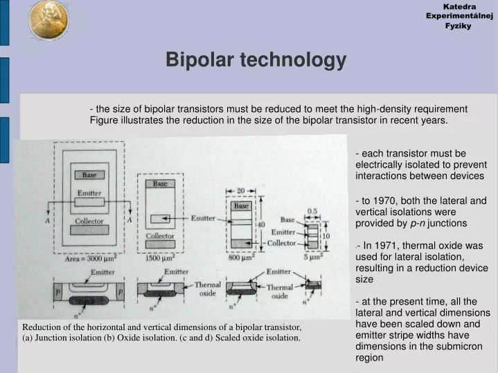
Bipolar technology. - the size of bipolar transistors must be reduced to meet the high-density requirement Figure illustrates the reduction in the size of the bipolar transistor in recent years. - each transistor must be electrically isolated to prevent interactions between devices.

E N D
Bipolar technology - the size of bipolar transistors must be reduced to meet the high-density requirement Figure illustrates the reduction in the size of the bipolar transistor in recent years. - each transistor must be electrically isolated to prevent interactions between devices • - to 1970, both the lateral and vertical isolations were provided by p-n junctions • - In 1971, thermal oxide was used for lateral isolation, resulting in a reduction device size • - at the present time, all the lateral and vertical dimensions have been scaled down and emitter stripe widths have dimensions in the submicron region Reduction of the horizontal and vertical dimensions of a bipolar transistor, (a) Junction isolation (b)Oxide isolation. (c and d)Scaled oxide isolation.
NPN type - the majority of bipolar transistor are n-p-n type because the higher mobility of minority carriers (electrons) in the base region results in higher-speed performance than can be obtained with p-n-p types • - figure shows a perspective view of an n-p-n type bipolar transistor, in which lateral isolation is provided by oxide walls (also reduce capacitance) • - vertical isolation is provided by the n+ -p junction • - let’s look the major process steps that are used to fabricate the device shown in figure
Cross-sectional view - the starting material is a p-type lightly doped (~1015 cm-3) - form a buried layer (minimize the series resistance of the collector) - deposit an n-type epitaxial layer oxide is removed and the wafer is placed in an epitaxial reactot - form the lateral oxide isolation region, a thin-oxide pad (~50nm) is thermally grown on the epitaxial layer, followed by a silicon-nitride deposition (~100nm) - next, the nitride-oxide layers and about half of the epitaxial layer are etched using a photoresist as mask - boron ions are then implanted into the exposed silicon areas
Cross-sectional view - the photoresist is removed and the wafer is placed in an oxidation furnace - next step is to form the base region, photoresist is used as a mask to protect the right half of the device; then boron ions are implanted to form the base regions another lithographic process removes all the thin-pad oxide except a small area near the center of the base region - form the emitter region; the base contact area is protected by a photoresist mask, then a low energy high arsenic dose (~1016cm-2) is removed; and a final metallization step forms the contacts to the base (emitter and collector)