Download
1 / 41
530 likes | 1.3k Vues
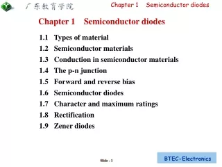
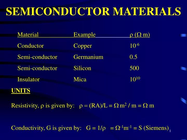
SEMICONDUCTOR MATERIALS. Material Example r ( m) Conductor Copper 10 -6 Semi-conductor Germanium 0.5 Semi-conductor Silicon 500 Insulator Mica 10 10. UNITS Resistivity, is given by: r = ( RA)/L = m 2 / m = m

E N D
SEMICONDUCTOR MATERIALS Material Exampler ( m) Conductor Copper 10-6 Semi-conductor Germanium 0.5 Semi-conductor Silicon 500 Insulator Mica 1010 UNITS Resistivity, is given by: r = (RA)/L = m2 / m = m Conductivity, G is given by: G = 1/r = -1m-1 = S (Siemens)
Germanium and Silicon Have the same crystal structure as diamond. Both can be made to purity levels of 1 in 10 billion (1 in 1010) Can significantly change properties by "doping". Just 1 in 106 impurity atoms can substantially increase the conductivity.
Atomic Structure The atom is composed of three basic particles: electrons, protons, and neutrons The neutrons and protons form the nucleus. The electrons revolve around the nucleus in a fixed orbit.
Atomic Structure Germanium has 32 orbiting electrons Silicon has 14 orbiting electrons (b) Bohr models of (a) Germanium and (b) Silicon The potential (ionization potential) required to remove any of these four valence electrons is lower than that required for any other electron in the structure.
Covalent Bonding The four valence electrons are bonded to four adjoining atoms. This bonding of atoms by sharing of electrons is called covalent bonding. Covalent bonding of the silicon atom
Intrinsic semi-conductors Silicon and germanium when carefully refined to reduce impurities to a very low level, are called intrinsic semiconductors. The conductivity for both pure materials is quite low. An increase in temperature causes a substantial increase in the number of free electrons, thus increasing conductivity. These materials thus have a negative temperature coefficient of resistance, (i.e. resistance decreases with temperature).
Energy Levels The more distant the electron from the nucleus the higher the energy state. Any electron that has left its parent atom to become a "free" electron has a higher energy state that any electron in the atomic structure. Energy levels for isolated atoms Between the discrete energy levels are gaps in which no electrons in the isolatedatomic structure can appear.
Energy Bands As the atoms of a material are brought closer together to form the crystal lattice structure the discrete levels of each atom will merge into bands.
Energy Bands There is a forbidden region between the valence band and ionization level (conduction band). Since, W = Q V 1 eV = (1.6 x 10⁻¹⁹ C) (1 V) = 1.6 x 10⁻¹⁹ J Since Eg is less for Ge than Si a larger number of valence electrons for Ge will have sufficient energy to cross the forbidden gap and become free. Thus Ge will have a greater conductivity than Si.
Extrinsic materials A semiconductor that has been subjected to "doping" is called an extrinsic material. Doping can be as low as 1 part in 10 million.
Extrinsic materials There are two types of extrinsic material: n type: impurity atoms have 5 valence electrons e.g. antimony, arsenic, and phosphorus p type: impurity atoms have 3 valence electrons e.g. boron, gallium, and indium
n type semiconductor There is an additional free electron for each impurity atom that is unassociated with any particular covalent bond. This is a "free" electron. The structure is electrically neutral since each Sb atom has an additional proton to balance the extra electron. Antimony impurity in n-type material
n type semiconductor Effect of donor impurities on the energy band structure A discrete energy level (the donor level appears in the forbidden gap). Since the Eg for this level is small electrons can easily be excited to the conduction band.
p type semiconductor There are now an insufficient number of electrons to complete the covalent bonds of the new lattice. The resulting vacancy is called a hole and is represented by a small circle or positive sign since the vacancy can accept a free electron. Again the structure is electrically neutral. Boron impurity in p type semiconductor
p type semiconductor Effect of acceptor impurities on the energy band structure A discrete energy level (the acceptor level appears in the forbidden gap). Since the Eg for this level is small electrons can easily be excited from the valence band, leaving holes in the valence band.
Majority and minority carriers Intrinsic state Free electrons in Ge or Si are due only to those few electrons in the valence band that have acquired enough energy to break the covalent bond or to the few impurities that could not be removed. Vacancies left behind in the valence band will be approximately same as number of free electrons.
Majority and minority carriers Extrinsic state For n type number of holes about same as intrinsic but far more free electrons. For p type number of holes far outweighs number of electrons. In n type material the electron is the majority carrier and the hole the minority carrier. In p type material the electron is the minority carrier and the hole the majority carrier
Semiconductor diode If the n type and p type are joined together the electrons and holes in the region of the junction combine forming a depletion layer.
Semiconductor diode This very thin layer (<10-3 mm) blocks drifting of electrons and holes. It acts as an insulator. In order to pass through the deletion zone, electrons need energy. Thus, the zone acts as a voltage barrier. This is the junction voltage which is 0.7 V for Si and 0.3 V for Ge.
Reverse Bias Electrons and holes are attracted away from the junction so it widens. Some minority carriers will cross the junction and will get a very small reverse saturation or leakage current IS.
Forward Bias If the battery voltage is greater than the junction voltage majority carriers will cross the junction and the depletion regions narrows considerably. As applied bias increases depletion region gets smaller and get a flood of electrons resulting in an exponential increase in the number of electrons crossing the barrier.
Diode Current vs Diode Voltage The current ID through a diode is calculated using: where: IS = reverse saturation current k = 11,600/ with = 1 for Ge and = 2 for Si at low current levels, = 1 for both at high current levels TK = TC + 273o
Zener Region As the reverse bias voltage across the diode increases reach a point where valence electrons absorb sufficient energy to reach ionization and get an avalanche breakdown. The voltage where this occurs is called the Zener Voltage, VZ. The maximum reverse bias potential that can be applied before entering the Zener region is called the peak inverse voltage (PIV) or peak reverse voltage (PRV).
Silicon vs Germanium PIV ratings for Si diodes are about 1000 V and about 400 V for Ge diodes. Si diodes can be used up to 200o C, Ge diodes up to 100o C. However, Si has a junction voltage of 0.7 V, and Ge has a junction voltage of 0.3 V.
Temperature Effects The reverse saturation current IS will double for every 10oC increase in temperature. Threshold voltage levels decrease with increasing temperature i.e forward characteristics become more ideal. Effect of temperature on Si diode characteristics
Temperature Effects Ge has much higher increase in IS with temperature increase. Thus Ge is not good at higher temperatures. Effect of temperature on Si diode characteristics
Diode Resistance As operating point of diode changes from one region to another resistance changes dramatically. (Very high in reverse bias, low in forward bias). Also, due to non-linear nature of curve resistance changes.
Load Line Analysis Diode and resistor are in a series circuit with DC power supply E. Using the Kirchoff voltage law: E = VD + VR = VD + IDR or, solving for ID, gives the load-line equation in terms of current: The diode characteristic curve is shown for forward bias at the left.
Load Line Analysis As the load-line equation is linear we need only two points: If VD = 0 then ID = E/R and if ID = 0 then VD = E this gives two points on the load line, and is shown in the next slide.
Load Line Analysis The point of intersection between the network line and the device curve is the operating point Q for the device and the circuit. The Q point is the quiescent point
Load Line Analysis Alternatively, can find Q mathematically by solving two equations: the equation for the device and, E = VD + IDR the load line equation This mathematics involves non-linear methods which is complex and time consuming. Load-line analysis is not only much simpler but provides a "pictorial" solution for finding the Q point values. We will use this method again for transistors later on in the course.
Example 1 To construct the load line need two points on axes. If VD = 0 then ID = E/R = 10V/1k = 10 mA and, if ID = 0 then VD = E = 10V
Example 1 The coordinates of the Q point are shown on the graph. For greater accuracy need a larger scale plot. • To obtain VR can use: • VR = I R = (9.25 mA)(1 k) = 9.25 V or, • VR = E – VD = 10 – 0.78 V = 9.22 V • Difference in results is due to the accuracy in reading the graph.
Example 2 Repeat analysis for Example 1 using R = 2 k If VD = 0 then ID = E/R = (10 V)/(2 k) = 5 mA and, if ID = 0 then VD = E = 10V. Construct a new load line as shown in next slide:
Example 2 Intersection of load line with curve gives new Q point. • Then, VR = I R = (4.6 mA)(2 k) = 9.2 V • or, VR = E – VD = 10 – 0.7 V = 9.3 V • Again, difference in results is due to the accuracy in reading the graph.
Example 3 • Repeat Example 1 using the practical diode model. Q point values obtained are almost the same.
Example 4 • Repeat Example 2 using the practical diode model. Q point values obtained are almost the same.
Example 5 • Repeat Example 1 using the ideal diode model. Q point values obtained are not as good.
Summary Practical model gives quite accurate results and is quite simple. Although even simpler, the ideal model is only good for when E >> VT. Throughout the course we will almost always use the practical model.