Download
1 / 20
200 likes | 350 Vues
p- type Si Homojunction Interfacial Workfunction Internal Photoemission Dual-Band Detector Responding in Near- and Far-Infrared Regions. G. Ariyawansa Department of Physics and Astronomy Georgia State University. Outline. Introduction Types of Junction Detectors Homojunction Detectors

E N D
p- type Si Homojunction Interfacial Workfunction Internal Photoemission Dual-Band DetectorResponding in Near- and Far-Infrared Regions G. AriyawansaDepartment of Physics and AstronomyGeorgia State University
Outline • Introduction • Types of Junction Detectors • Homojunction Detectors • Heterojunction Detectors Schottky Detectors Blocked Impurity Barrier (BIB) Detectors • Si HIWIP Detector Structure • Dual-Band Detection • Impurity Transitions and Hydrogenic Model • IVT Measurements and Arrhenious Calculations • Summary and Future Studies
Introduction • Multi-band IR detection is useful in numerous applications such as, • Mine Detection: The use of images in two different spectral bands can aid in the detection and reduce the number of false positives. • Military Applications: The NIR portion could be used to detect the muzzle flash while the FIR portion can be useful for determining troops and operating vehicles. • Remote Sensing: Taking the difference in the spectral information of the signal for the two bands. • Other applications: Environmental Monitoring, Medical Diagnosis, Space Astronomy Applications, Spectroscopy … • Interfacial workfunction detectors: • FIR detector designs • Broad response • Tailarable wavelength threshold • Dual-band detection
Types of Junction Detectors • Homojunction Detectors • Heterojunction Detectors • Schottky Detectors • Blocked Impurity Barrier (BIB ) Detectors
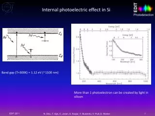
Three Types of Homojunction Detector Structures + Thermal n (Emitter) Diffusion i (Barrier) i D E E + C C n E Tunneling C D n h Field E F e Impurity Band Type I - Nd < Nc ( ECn+ >EF) Nd : Doping of Emitter Nc : Mott’s critical concentration D = (ECn+-EF) + DEC JAP 77, 915, (1995)
Three Types of Homojunction Detector Structures n h i E C D D E Field C F e Impurity Band + n C + i (Barrier) n (Emitter) Type II - Nc < Nd < N0 ( ECn+ < EF < ECi ) Nd : Doping concentration of the Emitter/ Absorber Nc : Mott’s critical concentration N0 : Critical concentration E D = Eci- EF E • Fermi level is above the conduction band edge of the emitter • Emitter becomes metallic • Infrared absorption is due to free carriers JAP 77, 915, (1995)
Three Types of Homojunction Detector Structures n e h E F Bias ++ n - - n i (n ) Type III - Nd > N0 ( EF > ECi ) Nd : Doping concentration of the Emitter/ Absorber N0 : Critical concentration • Fermi level is above the conduction band edge of the barrier • Conduction band edge of the Emitter and the barrier become degenerate • Space charge region at the n++ - i interface forms the barrier • Barrier height depends on the concentration and the applied field JAP 77, 915, (1995)
Si HIWIP- Detector Structure • Doping • Ntc = 1.5 X 1019 cm-3 • Ne = 3 X 1018 cm-3 • Nb = 1 X 1010 cm-3 • Nbc = 1.5 X 1019 cm-3
Dual-Band Detection • NIR response : Interband transitions in the Si barrier • FIR response : Intraband transitions in the structure
Near-IR Response • E2TO, E1TO : Phonon assisted exciton transitions at the bang edge.
Near-/Far- IR Dual Band Response @ 5.3 K • The NIR photons are absorbed in the barrier giving rise to a transition of carriers (electron-hole pair) between conduction and valence band of the GaAs barrier. • Incident MIR/FIR photons undergo free carrier absorption in the emitter. • Threshold wavelength varies with the applied bias
Near-/Far- IR Dual Band Response @ 30 K • Labeled peaks are related to impurity transitions of Boron in Si. • Numbers assigned are in meV and numbers in parenthesis are reported values. • The strength of the peak increases with the bias and the temperature.
IVT Measurements • BLIP temperature is 25 K at ± 0.9 V
Arrhenious Calculations • Arrhenious calculations are not valid out of the bias range from ~ -0.5V to 0.5V • This results consistent with spectral results.
Conclusion and Future Studies • A single emitter Si HIWIP dual-band detector can detect NIR and MIR/FIR radiation. • Interband transitions in Si lead to NIR response while FIR response is due to intraband transitions in the structure. • High performance of the detector demonstrate the potential applications where the detection in both NIR and FIR are important. • Future Studies >>>> • Developing a dual band detector covering UV and FIR regions. • Band tuning based on operational conditions.