Download
1 / 59
610 likes | 888 Vues
Digital System 數位系統. Xilinx FPGA Design Flow. Ping-Liang Lai ( 賴秉樑 ). Outline of FPGA Design Flow. Project Navigator 視窗介紹 設計流程 I: 以 Schematic 設計電路 建立新的專案 (Project) 以繪圖方式 (Schematic) 設計電路 功能模擬 (Functional Simulation) 的執行 Testbench 的產生 功能模擬 : 使用 Modelsim Simulator 晶片實作

E N D
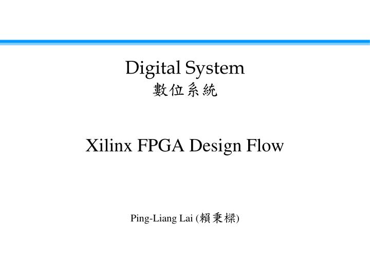
Digital System數位系統 Xilinx FPGA Design Flow Ping-Liang Lai (賴秉樑)
Outlineof FPGA Design Flow • Project Navigator 視窗介紹 • 設計流程I:以 Schematic 設計電路 • 建立新的專案 (Project) • 以繪圖方式 (Schematic) 設計電路 • 功能模擬 (Functional Simulation) 的執行 • Testbench 的產生 • 功能模擬: 使用 Modelsim Simulator • 晶片實作 • Implementation Constraints File 的執行 • Implementation Design • 時序模擬 (Timing Simulation) 的執行: 使用 Modelsim Simulator • Configuration 的執行 • 驗證電路 • 設計流程II: 以 Verilog 設計電路
Project Navigator 視窗介紹 (1/2) Multi-document Interface Source 視窗 Process Source 視窗 Transcript 視窗
Project Navigator 視窗介紹 (2/2) • Source 視窗 • Sources Tab • 專案 (Project) 的名稱、使用者的文件、FPGA/CPLD 的型號、設計流程與合成的工具與伴隨 Design View的設計來源檔案。 • Snapshot Tab • 顯示目前專案的所有 Snapshot,所謂 Snapshot 主要在儲存以前儲存過的 Project。 • Library Tab • 顯示目前所開啟的 Project 用到相關的 Library。 • Processes Source 視窗 • 顯示目前要處理的有效程序。 • Transcript 視窗 • Console, Error, Warning, Tcl Console, and Find in Files.
Outlineof FPGA Design Flow • Project Navigator 視窗介紹 • 設計流程I:以 Schematic 設計電路 • 建立新的專案 (Project) • 以繪圖方式 (Schematic) 設計電路 • 功能模擬 (Functional Simulation) 的執行 • Testbench 的產生 • 功能模擬: 使用 Modelsim Simulator • 晶片實作 • Implementation Constraints File 的執行 • Implementation Design • 時序模擬 (Timing Simulation) 的執行: 使用 Modelsim Simulator • Configuration 的執行 • 驗證電路 • 設計流程II: 以 Verilog 設計電路
建立新的專案 (1/8) • Step 1: File→ New Project 1 3 2
建立新的專案 (2/8) • 燒錄的 FPGA 晶片型號: Spartan 3 XC3S200-FT256
建立新的專案 (3/8) • Step 2: 增加一個新的 Source 檔,使用 Schematic 來設計。 1 2 3 4
建立新的專案 (4/8) • New Source Summary 1
建立新的專案 (5/8) • We only need one Source, so Next. 1
建立新的專案 (6/8) • We don’t need and have any Existing Sources, so Next. 1
建立新的專案 (7/8) • New Project Summary
建立新的專案 (8/8) 1. 檢查 Source 檔,與 Device 。 2. 開始編輯電路。
Outlineof FPGA Design Flow • Project Navigator 視窗介紹 • 設計流程I:以 Schematic 設計電路 • 建立新的專案 (Project) • 以繪圖方式 (Schematic) 設計電路 • 功能模擬 (Functional Simulation) 的執行 • Testbench 的產生 • 功能模擬: 使用 Modelsim Simulator • 晶片實作 • Implementation Constraints File 的執行 • Implementation Design • 時序模擬 (Timing Simulation) 的執行: 使用 Modelsim Simulator • Configuration 的執行 • 驗證電路 • 設計流程II: 以 Verilog 設計電路
Schematic 圖形編輯器 (1/5) • Schematic 快速鍵介紹 Add I/O Maker Add wire Add Symbol Add Net Name
Schematic 圖形編輯器 (2/5) • Step 3: Add → Symbol and Wire.
Schematic 圖形編輯器 (3/5) • Step 4: Add →IO Maker.
Schematic 圖形編輯器 (4/5) • Step 5: Add → Net name.
Schematic 圖形編輯器 (5/5) • Step 6: Tool Check schematic, and check no error and Save. 3 1 2
Outlineof FPGA Design Flow • Project Navigator 視窗介紹 • 設計流程I:以 Schematic 設計電路 • 建立新的專案 (Project) • 以繪圖方式 (Schematic) 設計電路 • 功能模擬 (Functional Simulation) 的執行 • Testbench 的產生 • 功能模擬: 使用 Modelsim Simulator • 晶片實作 • Implementation Constraints File 的執行 • Implementation Design • 時序模擬 (Timing Simulation) 的執行: 使用 Modelsim Simulator • Configuration 的執行 • 驗證電路 • 設計流程II: 以 Verilog 設計電路
功能模擬的執行 (1/12) • Step 7: Source for Behavioral Simulation,點選 fa (fa.sch),add new source,檔名為 fa_tbw。 1 2 3 4
功能模擬的執行 (2/12) • We only have one source, so Next. 1 2
功能模擬的執行 (3/3) • New Source Summary 1
功能模擬的執行 (4/12) 1 2 3
功能模擬的執行 (5/12) • Step 8: 輸入 input 的所有組合,n inputs → 2n input combinations.
功能模擬的執行 (6/12) • Step 9:Modelsim Simulator → Simulate Behavioral Model (Double click mouse left key 2 times). 1 2
功能模擬的執行 (7/12) • 叫出 Modelsim Simulator後,You can see “Error Loading”.
功能模擬的執行 (8/12) • Step 10: Select work → Compiler AND2, OR3, and XOR2. (file path: C://Xilinx/9.2i/ISE/verilog/src/unisims) 1 2 3 4 5
功能模擬的執行 (9/12) • Step 11: In fa_tbw, Right click → Simulate 1 2 3
功能模擬的執行 (10/12) • Step 12: Right Click “fa_tbw” to select Add → To Wave → All items in region. 1 3 4 2
功能模擬的執行 (11/12) • Behavioral Waveform Window
功能模擬的執行 (12/12) • Step 14: Run all, and Step 15: Zoom fit. 1 2
Outlineof FPGA Design Flow • Project Navigator 視窗介紹 • 設計流程I:以 Schematic 設計電路 • 建立新的專案 (Project) • 以繪圖方式 (Schematic) 設計電路 • 功能模擬 (Functional Simulation) 的執行 • Testbench 的產生 • 功能模擬: 使用 Modelsim Simulator • 晶片實作 • Implementation Constraints File 的執行 • Implementation Design • 時序模擬 (Timing Simulation) 的執行: 使用 Modelsim Simulator • Configuration 的執行 • 驗證電路 • 設計流程II: 以 Verilog 設計電路
Implementation Constraints File 的執行 (1/8) • Step16: Sources for “ Synthesis/Implementation “ • Step 17: 點選 fa.sch,Project→ New Source 1 2 3 4
Implementation Constraints File 的執行 (3/8) • Step 18: 點選 fa.ucf,User Constraints → Assign Package Pins. 1 2 3
Implementation Constraints File 的執行 (4/8) • Xilinx PACE 視窗
Implementation Constraints File 的執行 (5/8) • Step 19: 點選Package View,展開Design Browser 的 I/O Pins 2 1
Implementation Constraints File 的執行 (6/8) • Step 20: 找出 Spartan-3 FPGA XC3S200-FT256 的 Datasheet • Slide Switches • LEDs
Implementation Constraints File 的執行 (7/8) • 完成後,File Save。
Implementation Constraints File 的執行 (8/8) • 檢查 Edit Constraints (Text) 1 2
Outlineof FPGA Design Flow • Project Navigator 視窗介紹 • 設計流程I:以 Schematic 設計電路 • 建立新的專案 (Project) • 以繪圖方式 (Schematic) 設計電路 • 功能模擬 (Functional Simulation) 的執行 • Testbench 的產生 • 功能模擬: 使用 Modelsim Simulator • 晶片實作 • Implementation Constraints File 的執行 • Implementation Design • 時序模擬 (Timing Simulation) 的執行: 使用 Modelsim Simulator • Configuration 的執行 • 驗證電路 • 設計流程II: 以 Verilog 設計電路
Implement Design (1/6) • Step 21: Implement Design 1 2
Implement Design (3/6) • 可點選Place & Route → View/Edit Routed Design (FPGA Editor),來觀看實際上 LUT 配置的情形。 2 1
Implement Design (4/6) • FPGA 晶片資源利用報告 (Design Summary → Summary)
Implement Design (5/6) • Pinoout Report (Design Summary Pinout Report) 1 2
Implement Design (6/6) • 時序報告的檢視: Generate Post-Place & Route Static Timing → Analyze Post-Place & Route Static Timing. 1
Outlineof FPGA Design Flow • Project Navigator 視窗介紹 • 設計流程I:以 Schematic 設計電路 • 建立新的專案 (Project) • 以繪圖方式 (Schematic) 設計電路 • 功能模擬 (Functional Simulation) 的執行 • Testbench 的產生 • 功能模擬: 使用 Modelsim Simulator • 晶片實作 • Implementation Constraints File 的執行 • Implementation Design • 時序模擬 (Timing Simulation) 的執行: 使用 Modelsim Simulator • Configuration 的執行 • 驗證電路 • 設計流程II: 以 Verilog 設計電路
時序模擬 (Timing Simulation) • 與 Functional Simulation 相同的步驟。 1 2