Download
1 / 1
10 likes | 113 Vues
Structural Quantum Size Effects in Pb/Si(111) P. Czoschke, Hawoong Hong, M. Holt, L. Basile and T.-C. Chiang Department of Physics, University of Illinois at Urbana-Champaign 1110 W. Green St., Urbana, IL 61801. Introduction

E N D
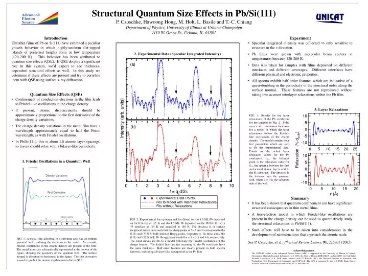
Structural Quantum Size Effects in Pb/Si(111) P. Czoschke, Hawoong Hong, M. Holt, L. Basile and T.-C. Chiang Department of Physics, University of Illinois at Urbana-Champaign 1110 W. Green St., Urbana, IL 61801 Introduction Ultrathin films of Pb on Si(111) have exhibited a peculiar growth behavior in which highly-uniform flat-topped islands of preferred heights form at low temperature (120-200 K). This behavior has been attributed to quantum size effects (QSE). If QSE do play a significant role in this system, we’d expect to see thickness-dependent structural effects as well. In this study we determine if these effects are present and try to correlate them with QSE using surface x-ray diffraction. • Experiment • Specular integrated intensity was collected only sensitive to structure in the z-direction. • Pb films were grown with molecular beam epitaxy at temperatures between 120-200 K. • Data was taken for samples with films deposited on different interfaces and different coverages. Different interfaces have different physical and electronic properties. • All spectra exhibit half-order features which are indicative of a quasi-doubling in the periodicity of the structural order along the surface normal. These features are not reproduced without taking into account interlayer relaxations within the Pb film. 2. Experimental Data (Specular Integrated Intensity) • Quantum Size Effects (QSE) • Confinement of conduction electrons in the film leads to Friedel-like oscillations in the charge density. • If present, atomic displacements should be approximately proportional to the first derivative of the charge density variations. • The charge density variations in the metal film have a wavelength approximately equal to half the Fermi wavelength, as with Friedel oscillations. • In Pb/Si(111), this is about 1.8 atomic layer spacings, so layers should relax with a bilayer-like periodicity. 3. Layer Relaxations FIG. 3: Results for the layer relaxations of the Pb overlayers for the samples in Fig. 2. Solid curves are continuous functions for a model in which the layer relaxations follow the Friedel-like oscillations of the charge density. The model contains four free parameters which are used to fit the experimental data. Points are the actual layer relaxation values for the Pb overlayers; i.e., the leftmost point is the relaxation value for d12, the spacing between the first and second atomic layers next to the Si substrate. The abscissa is the distance into the quantum well, where z = 0 is the substrate side of the well. 1. Friedel Oscillations in a Quantum Well • Summary • It has been shown that quantum confinement can have significant structural consequences in thin metal films. • A free-electron model in which Friedel-like oscillations are present in the charge density can be used to quantitatively study the structural relaxations in Pb/Si(111). • Such effects will have to be taken into consideration in the development of nanostructures that approach the atomic scale. • See P. Czoschke, et al., Physical Review Letters, 91, 226801 (2003) FIG. 2: Experimental data (points) and fits (lines) for (a) 8.5 ML Pb deposited on Si(111)-7x7 at 185 K and (b) 4.5 ML Pb deposited on the Pb/Si(111)-3 x 3 interface at 115 K and annealed to 180 K. The abscissa is in surface reciprocal lattice units such that the sharp peaks at l = 3 and 9 correspond to the (111) and (333) Si bulk-indexed Bragg peaks, respectively. In these units, the (111) and (222) bulk Pb Bragg peaks would be at l = 3.3 and 6.6, respectively. The solid curves are fits to a model following the Friedel oscillations of the charge density. The dashed lines are fits assuming all the Pb overlayers have the same thickness. Half-order features are clearly present in both spectra (arrows), indicating a bilayer-like superperiod in the Pb film. FIG. 1: A metal film adsorbed to a substrate acts like an infinite potential well confining the electrons in the metal. As a result, Friedel oscillations in the charge density are present in the film. The metal atoms are schematically represented at the bottom of the figure, showing the geometry of the quantum well. The surface normal (z-direction) is horizontal in the figure. The first derivative is used to predict the atomic displacements due to QSE. Acknowledgements The UNICAT facility at the Advanced Photon Source (APS) is supported by the University of Illinois at Urbana-Champaign, Materials Research Laboratory (U.S. DOE, the State of Illinois-IBHE-HECA, and the NSF), the Oak Ridge National Laboratory (U.S. DOE under contract with UT-Battelle LLC), the National Institute of Standards and Technology (U.S. Department of Commerce) and UOP LLC. The APS is supported by the U.S. DOE, Basic Energy Sciences, Office of Science under contract No. W-31-109-ENG-38.