Download
1 / 28
350 likes | 1.75k Vues
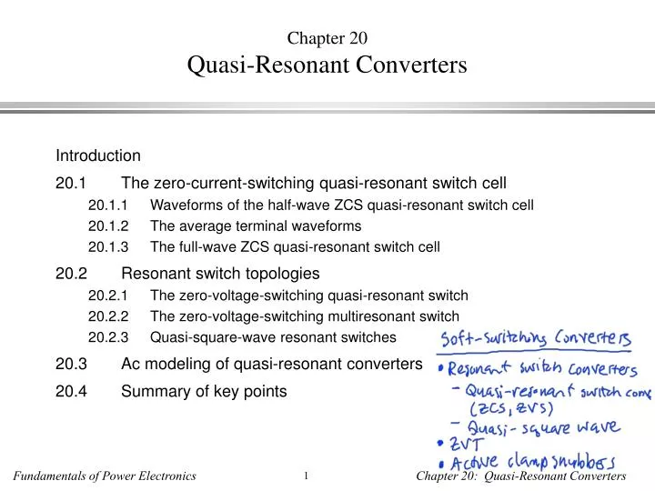
Chapter 20 Quasi-Resonant Converters. Introduction 20.1 The zero-current-switching quasi-resonant switch cell 20.1.1 Waveforms of the half-wave ZCS quasi-resonant switch cell 20.1.2 The average terminal waveforms 20.1.3 The full-wave ZCS quasi-resonant switch cell

E N D
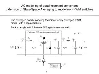
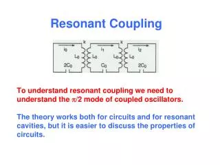
Chapter 20Quasi-Resonant Converters • Introduction • 20.1 The zero-current-switching quasi-resonant switch cell 20.1.1 Waveforms of the half-wave ZCS quasi-resonant switch cell 20.1.2 The average terminal waveforms 20.1.3 The full-wave ZCS quasi-resonant switch cell • 20.2 Resonant switch topologies 20.2.1 The zero-voltage-switching quasi-resonant switch 20.2.2 The zero-voltage-switching multiresonant switch 20.2.3 Quasi-square-wave resonant switches • 20.3 Ac modeling of quasi-resonant converters • 20.4 Summary of key points
Analysis result: switch conversion ratio µ Switch conversion ratio: with This is of the form
Characteristics of the half-wave ZCS resonant switch Switch characteristics: Mode boundary: Js ≤ 1
Buck converter containing half-wave ZCS quasi-resonant switch Conversion ratio of the buck converter is (from inductor volt-second balance): For the buck converter, ZCS occurs when Output voltage varies over the range
Boost converter example For the boost converter, Half-wave ZCS equations:
20.1.3 The full-wave ZCS quasi-resonant switch cell Half wave Full wave
Analysis: full-wave ZCS Analysis in the full-wave case is nearly the same as in the half-wave case. The second subinterval ends at the second zero crossing of the tank inductor current waveform. The following quantities differ: In either case, µ is given by
Full-wave cell: switch conversion ratio µ Full-wave case: P1 can be approximated as so
Full Wave Half Wave
Hard switching at turn-off of diodeConventional buck converter example (Fig. 20.1)
Zero-current switching at turn-off of diodeZVS quasi-resonant buck example (Fig. 20.2)
Zero-voltage switching at turn-off of diodeZVS quasi-squarewave buck example (Fig. 20.2)
Zero-current and zero-voltage switching • ZCS quasi-resonant switch: • Tank inductor is in series with switch; hence SW switches at zero current • Tank capacitor is in parallel with diode D2; hence D2 switches at zero voltage • Discussion • Zero voltage switching of D2 eliminates switching loss arising from D2 stored charge. • Zero current switching of SW: device Q1 and D1 output capacitances lead to switching loss. In full-wave case, stored charge of diode D1 leads to switching loss. • Peak transistor current is (1 + Js) Vg/R0, or more than twice the PWM value.
20.2 Resonant switch topologies Basic ZCS switch cell: SPST switch SW: • Voltage-bidirectional two-quadrant switch for half-wave cell • Current-bidirectional two-quadrant switch for full-wave cell • Connection of resonant elements: • Can be connected in other ways that preserve high-frequency components of tank waveforms
Connection of tank capacitor Connection of tank capacitor to two other points at ac ground. This simply changes the dc component of tank capacitor voltage. The ac high-frequency components of the tank waveforms are unchanged.
A test to determine the topologyof a resonant switch network • Replace converter elements by their high-frequency equivalents: • Independent voltage source Vg: short circuit • Filter capacitors: short circuits • Filter inductors: open circuits • The resonant switch network remains. If the converter contains a ZCS quasi-resonant switch, then the result of these operations is
20.2.1 The zero-voltage-switchingquasi-resonant switch cell When the previously-described operations are followed, then the converter reduces to A full-wave version based on the PWM buck converter:
ZVS quasi-resonant switch cell Switch conversion ratio Tank waveforms half-wave full-wave ZVS boundary A problem with the quasi-resonant ZVS switch cell: peak transistor voltage becomes very large when zero voltage switching is required for a large range of load currents.
20.2.2 The ZVS multiresonant switch When the previously-described operations are followed, then the converter reduces to A half-wave version based on the PWM buck converter:
20.2.3 Quasi-square-wave resonant switches ZCS When the previously-described operations are followed, then the converter reduces to ZVS
A quasi-square-wave ZCS buck with input filter • The basic ZCS QSW switch cell is restricted to 0 ≤ µ ≤ 0.5 • Peak transistor current is equal to peak transistor current of PWM cell • Peak transistor voltage is increased • Zero-current switching in all semiconductor devices
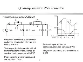
A quasi-square-wave ZVS buck • The basic ZVS QSW switch cell is restricted to 0.5 ≤ µ ≤ 1 • Peak transistor voltage is equal to peak transistor voltage of PWM cell • Peak transistor current is increased • Zero-voltage switching in all semiconductor devices