Download
1 / 27
420 likes | 894 Vues
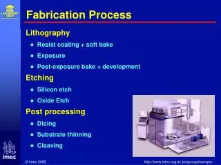
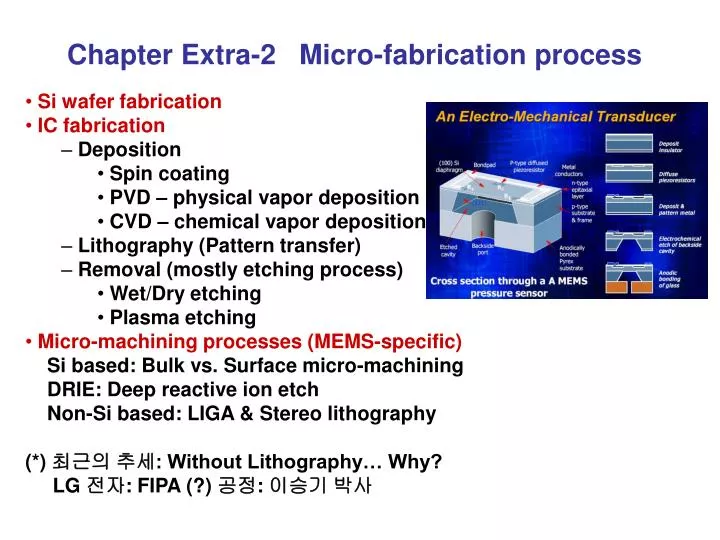
Chapter Extra-2 Micro-fabrication process. Si wafer fabrication IC fabrication Deposition Spin coating PVD – physical vapor deposition CVD – chemical vapor deposition Lithography (Pattern transfer) Removal (mostly etching process) Wet/Dry etching Plasma etching

E N D
Chapter Extra-2 Micro-fabrication process • Si wafer fabrication • IC fabrication • Deposition • Spin coating • PVD – physical vapor deposition • CVD – chemical vapor deposition • Lithography (Pattern transfer) • Removal (mostly etching process) • Wet/Dry etching • Plasma etching • Micro-machining processes (MEMS-specific) • Si based: Bulk vs. Surface micro-machining • DRIE: Deep reactive ion etch • Non-Si based: LIGA & Stereo lithography • (*) 최근의 추세: Without Lithography… Why? • LG 전자: FIPA (?) 공정: 이승기 박사
Example of MEMS products Surface micro-machining product LIGA product
Wafers Deposition Lithography Etch Chips Process flow of IC & MEMS fabrication • Processes of IC and MEMS are almost same • Process complexity/yield depends on repetition of central loop
Silicon wafer fabrication Czochralski process: widely-used to make single crystal Si
Silicon wafer fabrication – slicing & polishing CMP is used.. Why? Smart cutting process?
Deposition processes • - Issues of deposition : Compatibility, Conformability • - Process: • Spin casting/Spin coating • PVD – physical vapor deposition • CVD – chemical vapor deposition • Barrier layer formation • Materials • - SiO2 : most common • - Si3N4, polysilicon, metals etc… • Process • - Thermal oxidation, Evaporation, Sputtering, CVD
Spin Casting/Coating • Viscous liquid is poured on center of wafer • Wafer spins at 1000-5000 RPM for ~30s (thickness control) • Baked on hotplate 80-500oC for 10-1000s (volume reduction by 1/2) • Application of etchants and solvents, rinsing • Deposition of polymers, sol-gel precursors (SOG)
Physical Vapor Deposition - Evaporation • (1) Heating target with desired material to evaporate • in the vacuum chamber • (2) Thin film is formed on the substrate • Disadvantage: high temperature, high vacuum substrate Vacuum E-beam target heating
+ substrate atoms Plasma RF source Ar+ target - Physical Vapor Deposition - Sputtering • Sputtered metals and dielectrics • Argon plasma sputters material (small #s of atoms) off target • Ejected material takes ballistic path to wafers • Typically line-of-sight from a distributed source • Requires high vacuum depending on material Mechanism: Physical process by impact of ions (plasma state) (1) impacting target surface with accelerated ions (Ar+) (2) knocking out atoms from the target surface (3) transporting atoms to the substrate for deposition (4) spin the substrate to achieve uniform thickness
Wafers To exhaust system N2 H2 HCl Dopant+ H2 Susceptor SiCl4+ H2 Chemical Vapor Deposition - CVD • Process • Gas phase is injected into the chamber • Thermal decomposition and/or reaction • of gaseous compounds occur on the substrate surface • (3) Desired material is deposited directly from the gas phase • to form thin layer
Lithography • Pattern transfer: transferring a mask pattern onto wafer • Procedure • Deposit barrier layer (SiO2, Si3N4, metal, etc.) • Coat with PR • Soft baking (curing) • Align mask • Expose pattern and develop PR • Hard baking and Etching • Remove PR • Issues: Light source, Barrier layer, Mask, PR, Etching
Light source • UV, EUV (Extreme UV), X-ray, e-beam, etc. • - Shorter wavelength for higher resolution (e.g. UV) • - UV is difficult to use for nano-scale • due to diffraction • - X-ray or electron beam or EUV for finer resolution • (on-going research topic)
Etching process • - Classification: (Wet vs. Dry), (Isotropic vs. Anisotropic) • - Wet vs. Dry etching • Wet etching : liquid etchant • Dry etching : gas or plasma • Physical vs. Chemical • Plasma, Sputter, RIE • - Issues of etching : Anisotropy, Selectivity
<100> <111> anisotropic 54.7 mask Silicon Substrate undercut isotropic Isotropic vs. Anisotropic etching • Isotropic etchants etch at the same rate in every direction Anisotropic etching of Si
Bulk micro-machined cavities • Anisotropic KOH etch (upper left) • Isotropic plasma etch (upper right) • Isotropic BrF3 etch • with compressive oxide (lower right)
Reactive Ion Etching (RIE) Principle : Plasma is struck in the gas mixture and ions accelerated toward the substrate Reaction occurs on the surface (chemical) Impact of ion is similar to sputter etching (physical) Controlling balance between chemical and physical Physical : Anisotropic Chemical : Isotropic Deep RIE (DRIE) : altering two gas compositions High aspect ratio of 50:1, High etching rate
MEMS-specific fabrication processes • MEMS utilizes IC fabrication process for electric circuit, • MEMS-specific process for mechanical structure. • Bulk micro-machining • Surface micro-machining • Deep reactive ion etching (DRIE) • LIGA • Other materials/processes • Terminology • MEMS (미국) • Micro-machining (일본) • Micro system (EU)
Bulk & Surface micro-machining, DRIE & LIGA • Bulk micro-machining involves removing material • from silicon wafer itself. • Typically wet etched • Traditional MEMS industry • Artistic design, inexpensive equipment • Surface micro-machining leaves the wafer untouched, • but adds/removes additional layers above the wafer surface. • First widely used in 1990s. • Typically plasma etched • IC-like design philosophy, relatively expensive equipment • Deep Reactive Ion Etching (DRIE) removes substrate • but looks like surface micromachining.
Bulk vs. Surface micro-machining Bulk micro-machining bonding Surface micro-machining
Effects of residual stress Example of Bad Luck !!
DRIE and LIGA DRIE DRIE and LIGA: for high aspect ratio products but different process LIGA
LIGA process • LIthographie Galvanoformung Adformung • (Lithography/Electroplating/Plastic molding) • Developed during 1980s at Research Center Karlsruhe • Possible to produce microstructures with very highaspect ratios (up to 100), • very small structures (in the submicron range), • and with very smooth walls (surface roughness < 50 nm) • To manufacture a tool in a molding step to replicate the microstructure of polymer • Processes : Basic LIGA • SLIGA (Sacrificial LIGA) • LIGA-like process
Basic LIGA process Lithography/Electroplating/Plastic molding
Summary Think of SCALE-BRIDGING concept (micro-macro, nano-micro) Think of applying your major to micro-scale !