Download
1 / 19
260 likes | 542 Vues
NANO-Lithography. Name : DEKONG ZENG EE235 Spring 2007. Recent progress in high resolution lithography Daniel Bratton, Da Yang, Junyan Dai and Christopher K. Ober* Materials Science and Engineering, Cornell University, Ithaca, NY 14853, USA. All material gathered from Public Domain.

E N D
NANO-Lithography Name : DEKONG ZENG EE235 Spring 2007 Recent progress in high resolution lithography Daniel Bratton, Da Yang, Junyan Dai and Christopher K. Ober* Materials Science and Engineering, Cornell University, Ithaca, NY 14853, USA All material gathered from Public Domain
Outline • Photo-Lithography • Immersion Lithography • EUV Lithography • Two-Photon 3D Lithography • NANO-imprint Lithography • NANO-fabrication with Block Copolymers
Photolithography • Abbe (critical) illumination: • ---intensity in each location on reticle is determined by corresponding location in light source。 • Köhler illumination • ---intensity in each location on reticle is integral local source intensities。
Lithography Road Map Cost of a stepper today: $20M!
Improvement of immersion lithography At same CD : improvements in DOF Improvements in resolution The resolution enhancement from immersion lithography is therefore about 30-40% (depending on materials used), or about one technology node. The depth of focus, is also 40-70% better (proportional to the refractive index of the imaging medium considered) than a corresponding "dry" tool at the same resolution
Immersion lithography system Immersion lithography: $30M!! Fluid: 193nm water 157nm polyfluoropolyether high index fluids desired.
Immersion lithography Defects Contribution of Defects Images of Defects
Issues with Immersion Lithography Very big lenses (hence expensive) !! Field size reduction ? Mechanical issues and hydrodynamics Bubble formation disturbing the image Stage vibrations transferred to lens Heating of immersion liquid upon exposure New defect mechanisms at wafer level Interaction of photo resist with immersion liquid Fluid contamination Polarization effects degrading contrast
EXTREME ULTRAVIOLET (EUV) Lithography • A laser is directed at a jet of xenon gas. When the laser hits the xenon gas, it heats the gas up and creates a plasma. • Once the plasma is created, electrons begin to come off of it and it radiates light at 13 nanometers, which is too short for the human eye to see. • The light travels into a condenser, which gathers in the light so that it is directed onto the mask. • A representation of one level of a computer chip is patterned onto a mirror by applying an absorber to some parts of the mirror but not to others. This creates the mask. • The pattern on the mask is reflected onto a series of four to six curved mirrors, reducing the size of the image and focusing the image onto the silicon wafer. Each mirror bends the light slightly to form the image that will be transferred onto the wafer.
(EUV) Lithography Gas discharged plasma Laser produced plasma This entire process has to take place in a vacuum because these wavelengths of light are so short that even air would absorb them. Additionally, EUVL uses concave and convex mirrors coated with multiple layers of molybdenum and silicon -- this coating can reflect nearly 70 percent of EUV light at a wavelength of 13.4 nanometers. The other 30 percent is absorbed by the mirror. Without the coating, the light would be almost totally absorbed before reaching the wafer. The mirror surfaces have to be nearly perfect; even small defects in coatings can destroy the shape of the optics and distort the printed circuit pattern, causing problems in chip function.
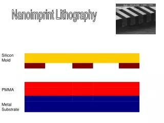
Commerical nanoimprinter: $0.5-1.6M Step-and-Flash IMPRINT Lithography (SFIL) • Lower forces: 100 kPa • No heating, no cooling • Longer lifetime, faster imprint • Sub 5-nm demonstrated • Issues: • Productionof templates • Defectcontrol • Small throughput • Materials